Zero-delay buffer circuit for a spread spectrum clock system and method therefor

a spread spectrum clock and buffer circuit technology, applied in the direction of generating/distributing signals, digital transmission, pulse automatic control, etc., can solve the problems of jitter problem, skew problem in the related art ssc technique, and improvement of the emi limit clock frequency in the related ar

Inactive Publication Date: 2006-01-31
ANAPASS
View PDF19 Cites 53 Cited by
  • Summary
  • Abstract
  • Description
  • Claims
  • Application Information

AI Technical Summary

Benefits of technology

[0015]An object of the invention is to solve at least the related art proble...

Problems solved by technology

As a result, EMI limits clock frequency improvements in the related art.
However, the related art SSC technique has various disadvantages.
For example, a jitter problem occurs due to a difference in period between a maximum frequency and a minimum frequency.
A skew problem also exists in the related art SSC technique due to a period difference between the frequency-modulated clock signal and the output clock signal.
The cumulative effect...

Method used


Image

  • Zero-delay buffer circuit for a spread spectrum clock system and method therefor
  • Zero-delay buffer circuit for a spread spectrum clock system and method therefor
  • Zero-delay buffer circuit for a spread spectrum clock system and method therefor

Examples


Embodiment Construction

[0048]FIG. 8 illustrates a block diagram of a spread spectrum clocking (SSC) clock system circuit according to a preferred embodiment of the present invention. A motherboard 83, a SSC generator 78, a PLL circuit 81 and a CPU 77 are included. A peripheral board 75 includes a zero-delay clock buffer circuit 68 having a delay-locked loop (DLL) circuit 69. The zero-delay clock buffer circuit 68 receives a frequency-modulated clock signal from the SSC generator 78 and outputs an output clock signal to a peripheral device (e.g., SDRAM, accelerated graphics port, etc.) 76. The DLL circuit 69 includes a phase detector 71, a charge pump 72, a loop filter 73, and a voltage controlled delay-chain (VCDC) circuit 74

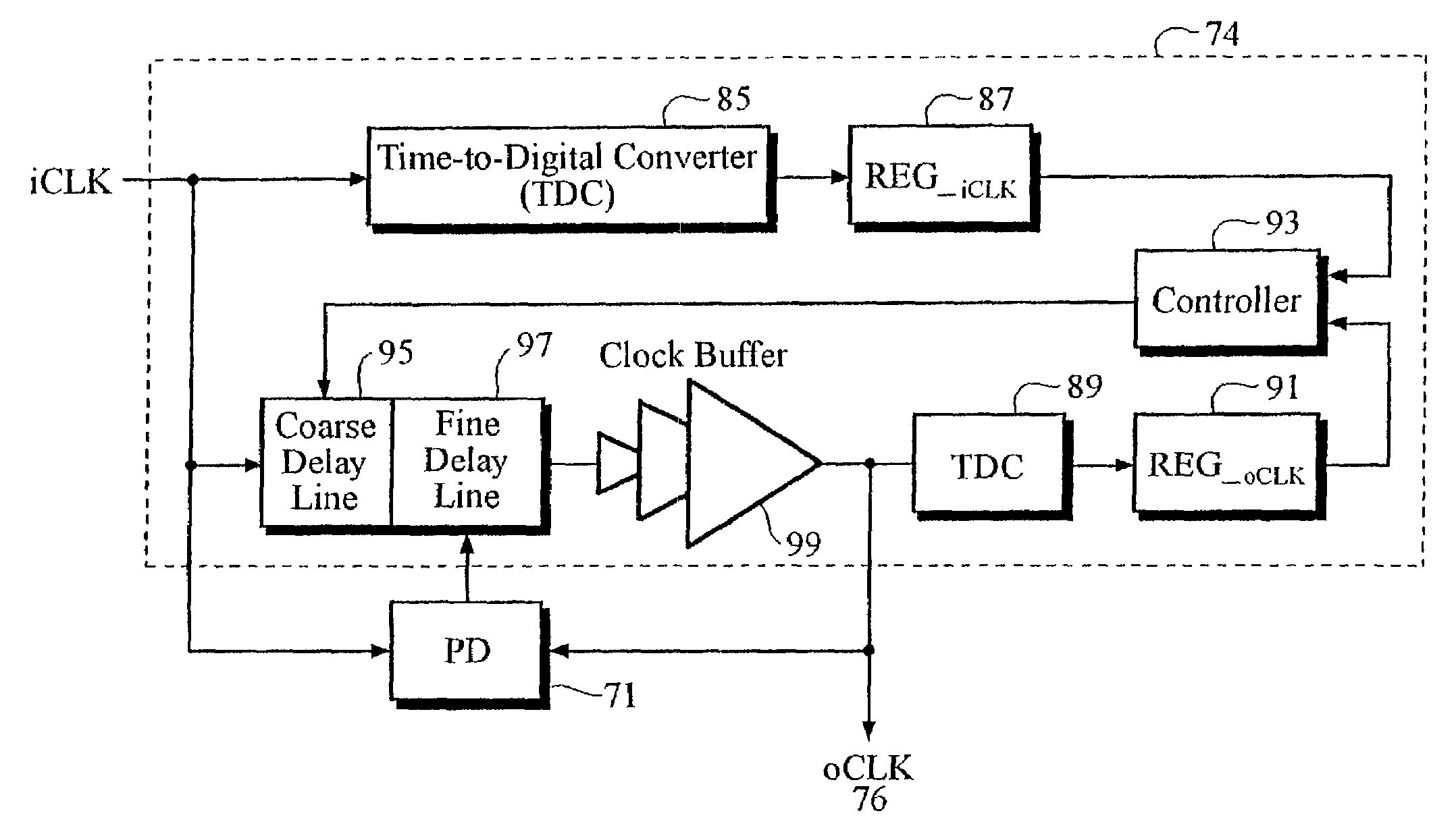
[0049]FIG. 9 illustrates a block diagram of the voltage controlled delay-chain (VCDC) circuit 74 according to the preferred embodiment of the present invention. The VCDC circuit 74 includes a first time-to-digital converter (TDC) 85 coupled to a first register 87, and a second TDC 89 ...


PUM


Abstract

A clock recovery circuit and a method for reducing electromagnetic emission (EMI) and increasing an attainable clock frequency includes a spread spectrum clock (SSC) generator that receives an input clock signal and generates a frequency-modulated clock signal, and a zero-delay buffer circuit that receives and buffers said modulated clock frequency signed to generated an output clock signal. The frequency-modulated clock signal and the output clock signal are phase-aligned such that there is no phase difference between the output clock signal and the modulated frequency clock signal. The clock recovery circuit also includes a delay-locked loop (DLL) circuit that reduces related art jitter and skew characteristics, and a phase detector circuit that eliminates phase ambiguity problems of a related art phase detector.

Description

[0001]This application is a Continuation of application Ser. No. 09 / 442,751 filed Nov. 18, 1999 now U.S. Pat. No. 6,731,667.BACKGROUND OF THE INVENTION[0002]1. Field of the Invention[0003]The present invention relates to a zero-buffer circuit for a spread spectrum clock (SSC) system and a method therefor and more specifically, to a zero-delay buffer circuit having a delay-locked loop (DLL) based zero-delay buffer.[0004]2. Background of the Related Art[0005]In a related art of improving computer system efficiency, it is desirable to increase a processing speed by operating a central processing unit (CPU) at a higher frequency by increasing a clock frequency. An increase in clock frequency increases a frequency of the computer system, as peripherals (e.g., memory, graphic card) can also operate at a higher frequency. However, as the clock frequency increases, electromagnetic emission (EMI) increases due to an increased peak amplitude. As a result, EMI limits clock frequency improvemen...

Claims


Application Information

Patent Timeline
IPC IPC(8): H03D3/24G06F1/04G06F1/10H03L7/081H03L7/07H03L7/089H03L7/23H04B15/04H04L7/033
CPCG06F1/10H03L7/07H03L7/0805H03L7/23H04B15/04H03L7/0812H04B2215/067H04B2215/064H03L7/0891H03L7/0818H03L7/0816H03L7/0814G06F1/04
Inventor LEE, KYEONGHOPARK, JOONBAE
Owner ANAPASS
Why Eureka
Try Eureka