
Steady-state non-equilibrium distribution of free carriers and photon energy up-conversion using same

a free carrier and non-equilibrium technology, applied in the direction of instruments, material analysis through optical means, optical elements, etc., can solve the problems of limited application usefulness, high cost and complexity of hybrid technologies, and intense expenditure of resources to improve, so as to improve the detection and processing of optical signals, the effect of high efficiency

Inactive Publication Date: 2006-02-07
SIRICA CORP
View PDF7 Cites 35 Cited by
  • Summary
  • Abstract
  • Description
  • Claims
  • Application Information

AI Technical Summary

Benefits of technology

[0065]In another related aspect, the integration of a light converter formed in accordance with the present invention with a conventional silicon-based photo-detector or a conventional silicon imaging circuit, such as a CMOS or CCD device, offers a high performance, photon (quantum), un-cooled, IR detector with an optically tunable spectral range that is formed from entirely silicon-based materials.
[0066]Consistent with foregoing, the present invention also provides specialized media adapted to implement improved optical signal detection and processing. In general, this media is formed from mesoscopic sized particles formed from a semiconductor or metal and provided within a matrix formed from a wide-bandgap semiconductor or dielectric material, such as SiO2, Si3N4, or amorphous silicon. When operatively assembled to receive an optical input signal and an optical pumping signal, the specialized media produces a highly efficient, double-photon induced photoluminescence.

Problems solved by technology

However, the indirect band-gap nature of silicon greatly limits its usefulness in applications like optoelectronic and photonic devices.
As a result, the merger of silicon-based electronics with non-silicon-based photonics has largely required the development of hybrid technologies that are often expensive and complicated to produce.
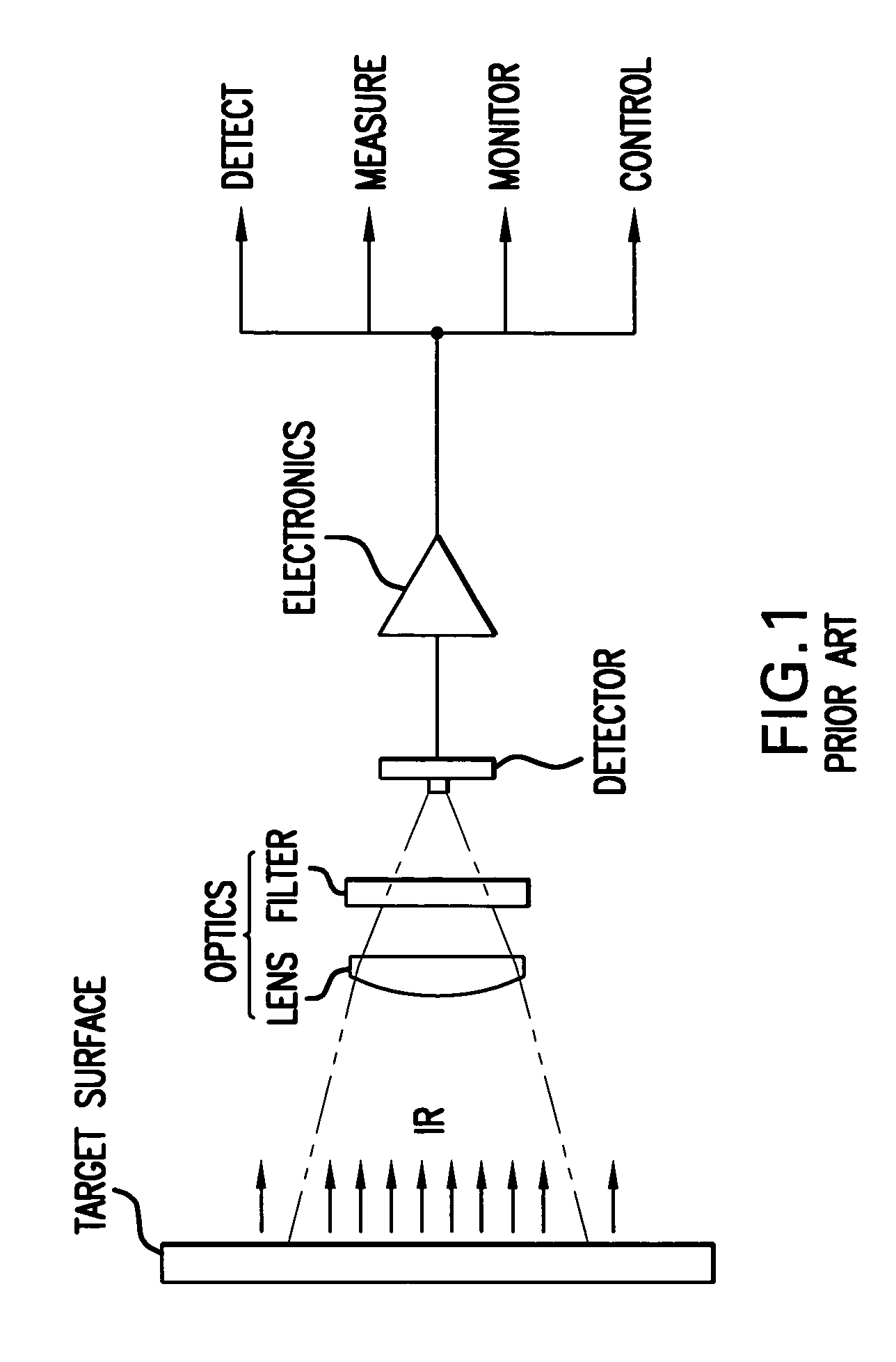
Since at least the 1970's, the promise of IR imaging has resulted in an intense expenditure of resources to improve IR detection capabilities (i.e., create IR photodetectors having improved detectivity and response time).
Being locked into either the first or the second thermal imaging band is a significant performance limitation attributable to conventional IR imaging system, regardless of the actual technology enabling IR detection.
Currently, multi-spectral systems rely on cumbersome imaging techniques that either disperse the optical signal across multiple IR FPAs or use a filter wheel to spectrally discriminate the image focused on a single FPA.
Consequently, these approaches are expensive in terms of size, complexity, and cooling requirements.
Infrared imaging systems do not actually sense warmth or cold like a thermometer.
Cooling requirements are the main obstacle to the more widespread use of IR systems based on semiconductor photodetectors making them bulky, heavy, expensive and inconvenient to use.
The reason for this disparity is that thermal detectors are popularly believed to be rather slow and insensitive in comparison with photon detectors.
As a result, the worldwide effort to develop thermal detectors was extremely small relative to that of photon detectors.
low sensitivity, requiring elaborate calibration and costly corrective electronics;
uniformity issues caused by the required combination of exotic materials;
difficult manufacturing processes including many steps and low device yields;
difficult maintenance issues and high power consumption; and,
Many of the disadvantages associated with conventional photon IR detectors are notable.
Indeed, these disadvantages have thus far largely overwhelmed the remarkable detection performance offered by photon IR detectors in all but the highest-end and most costly applications.
Large format arrays are most difficult to obtain given the low yields and the often non-uniform nature of the individual photon detectors.
This lack of compatibility with the mature field of silicon-based semiconductor manufacturing, together with the enormous burden (financial, maintenance, and technical) of a providing a sophisticated, external cooling system lead to the implementation of very expensive and often bulky IR detection systems.
However, these devices still suffer from a relatively large element size and slow response speeds.
Further, complex MEMS (micro-electromechanical) process techniques are implicated in the fabrication of these devices.
Low operation temperature is a fundamental limitation for QWIPs based on type III–V semiconductor materials.
This is due to the high strength of the longitudinal optical phonons within these materials, which results in a very strong thermal excitation of the electrons.
Therefore, such structures are characterized by large dark current and noise.
An additional drawback of QWIPs lies in the fact that they cannot detect normally incident light because of the ‘quantum mechanical polarization rule’ that requires an electric field component perpendicular to the layer planes of the quantum well structure.
Consequently, QWIPs have low quantum efficiency and require a long integration time for signals to achieve appropriate detectivity.
However, growth techniques for quantum dot structures are still in an early research and development state and quantum dot technology is far from maturity.
Problems relating to the control of dot density, size, and shape uniformity, as well as process stability and repeatability, still pose serious challenges.
This Hobson's choice between performance and cost in the field of IR imaging systems is just one result of the general lack of competent silicon-based optoelectronic devices.
However, silicon-based technologies are widely recognized for their poor performance in optical applications.

Method used


Image

  • Steady-state non-equilibrium distribution of free carriers and photon energy up-conversion using same
  • Steady-state non-equilibrium distribution of free carriers and photon energy up-conversion using same
  • Steady-state non-equilibrium distribution of free carriers and photon energy up-conversion using same

Examples


Embodiment Construction

)

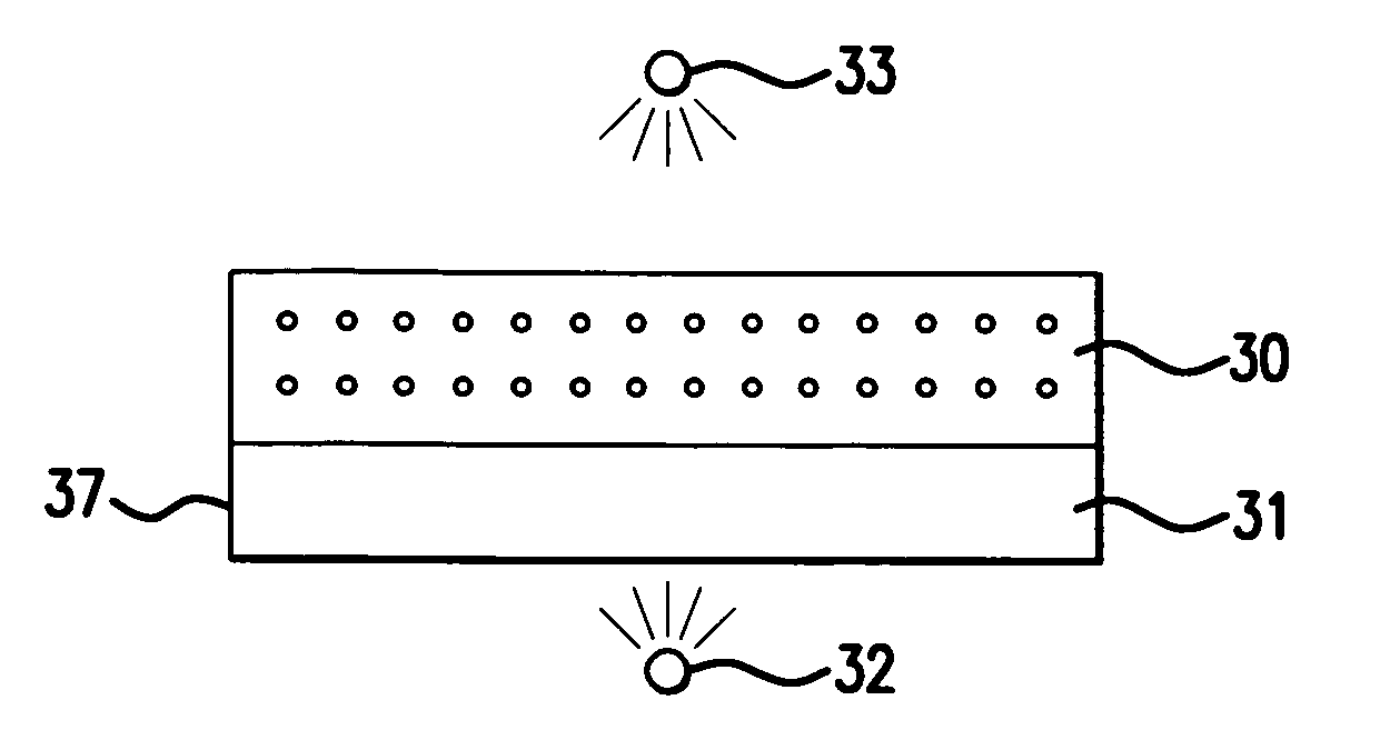
[0079]Within one exemplary embodiment of the present invention, a Steady-State Non-Equilibrium Distribution (“SNED”) of free carriers is created in a specialized media generally referred to hereafter as a “composite structure.” Additionally or alternatively, free carriers induced within the composite structure are confined in mesoscopic sized regions that are separated from a surrounding wide-bandgap material by an energetic barrier. The so-called “height” of the energetic barrier is a measurement of the energy required for a free carrier to overcome the barrier and penetrate from a mesoscopic sized region into the surrounding wide-bandgap material. The height is determined by a difference in electron affinities as between the components forming the composite structure and the number of surface states on the boundaries between these components.

[0080]“Free carriers” are charged carriers able to move freely through a material, as compared with other carriers bound up within the atomi...


PUM

PropertyMeasurementUnit
sizeaaaaaaaaaa
sizeaaaaaaaaaa
sizeaaaaaaaaaa

Abstract

Methods and specialized media adapted to the formation of a steady-state, non-equilibrium distribution of free carriers using mesoscopic classical confinement. Specialized media is silicon-based (e.g., crystalline silicon, amorphous silicon, silicon dioxide) and formed from mesoscopic sized particles embedded with a matrix of wide-bandgap material, such as silicon dioxide. An IR to visible light imaging system is implemented around the foregoing.

Description

[0001]This application claims the benefit of U.S. Provisional Application No. 60 / 477,752 filed Jun. 12, 2003.BACKGROUND OF THE INVENTION[0002]1. Field of the Invention[0003]The present invention provides specialized media and related methods whereby a photo-induced, Steady-State, Non-Equilibrium Electron Distribution (“SNED”) of free carriers is developed using Mesoscopic Classical Confinement (“MCC”). The photo-induced SNED of free carriers using MCC finds application across a broad range of technical fields, including as examples, infrared (IR) radiation detection and related imaging systems, light modulation, optical switching, wave-division multiplexing, optical amplifiers, lasers, data memories, and color displays.[0004]2. Description of the Related Art[0005]Advances in materials science have greatly enhanced our ability in recent years to engineer man-made materials with specific physical properties by creating different structural composites of useful materials such as semico...

Claims


Application Information

Patent Timeline
Patent Type & Authority Patents(United States)
IPC IPC(8): H01L31/00G02F1/01G02F1/355G02F2/02H01LH01L21/00
CPCB82Y20/00G02F1/353G02F2/02H01L31/02162G02B2006/12038G02F1/3556G02F2202/36G02F2203/11H01L27/1462H01L27/14649G02F2202/10H01L31/00
Inventor GARBER, VALERYBASKIN, EMANUELEPSTEIN, ALEXANDERFAYER, ALEXANDERSPEKTOR, BORIS
Owner SIRICA CORP
Learn More