Method for fabricating a transistor configuration including trench transistor cells having a field electrode, trench transistor, and trench configuration

a transistor and configuration technology, applied in the direction of electrical equipment, semiconductor devices, semiconductor/solid-state device details, etc., can solve the problems of disadvantageous increase in the on resistance rsub>ds(on)/sub>, and the stability of the channel and source structure, so as to improve the range of available process steps, reduce the gate-source breakdown voltage, and reduce the effect of gate-source capacitan

Active Publication Date: 2006-02-28
INFINEON TECH AG
View PDF11 Cites 120 Cited by
  • Summary
  • Abstract
  • Description
  • Claims
  • Application Information

AI Technical Summary

Benefits of technology

[0029]Therefore, it is an object of the invention to provide a method for fabricating a transistor configuration including trench transistor cells having a field electrode, a trench transistor, and a trench configuration, in which the variability of the available process steps is increased compared with known methods and / or the formation of channel and source zones is largely independent of subsequent process steps. In this case, the intention is to enable the gate electrode and / or the field electrode to be led from the trenches over the substrate surface without losses in the dielectric strength of the transistor configuration, and the intention is to provide a trench transistor cell and a transistor configuration having a low gate-source capacitance and a high gate-source breakdown voltage.

Problems solved by technology

What is disadvantageous about the known methods for fabricating a trench MOS power transistor having gate and field electrodes disposed in trenches is, inter alia, the fact that, as a result of the early doping of channel and source zones, subsequent process steps influence the formation of the doped zones and the variability of subsequent process steps is restricted in favor the stability of the structure of channel and source zones.
In the case of such transistor configurations, even slight subsequent influences on the fashioning of the channel zone lead to a disadvantageous increase in the on resistance RDS(on).

Method used


Image

  • Method for fabricating a transistor configuration including trench transistor cells having a field electrode, trench transistor, and trench configuration
  • Method for fabricating a transistor configuration including trench transistor cells having a field electrode, trench transistor, and trench configuration
  • Method for fabricating a transistor configuration including trench transistor cells having a field electrode, trench transistor, and trench configuration

Examples


examples

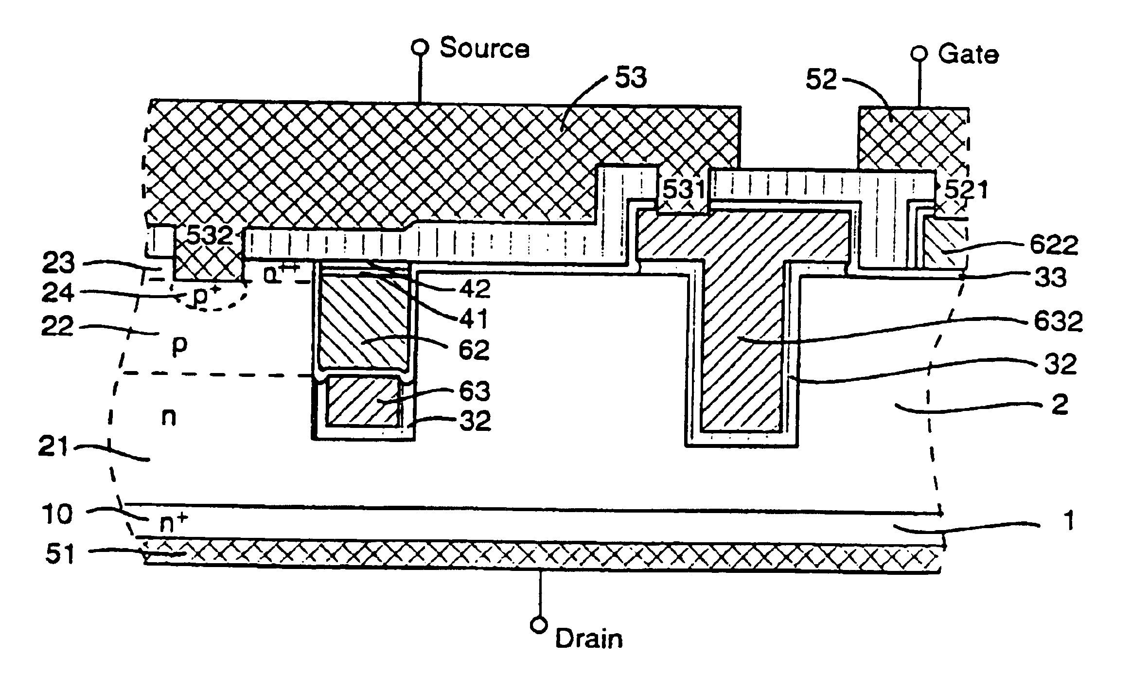
[0156]In all the examples below, the order of some steps, for example of the implantation operations, may vary. The gate electrode may include a plurality of layers or be reinforced in sections with a highly conductive material. In the region of the trench, the gate electrode may also project above the silicon surface p-channel transistors and IGBTs are also possible. The process sequence may be inserted into an IC process in which the drain zone is led to the substrate surface via an n-type sinker.

example a

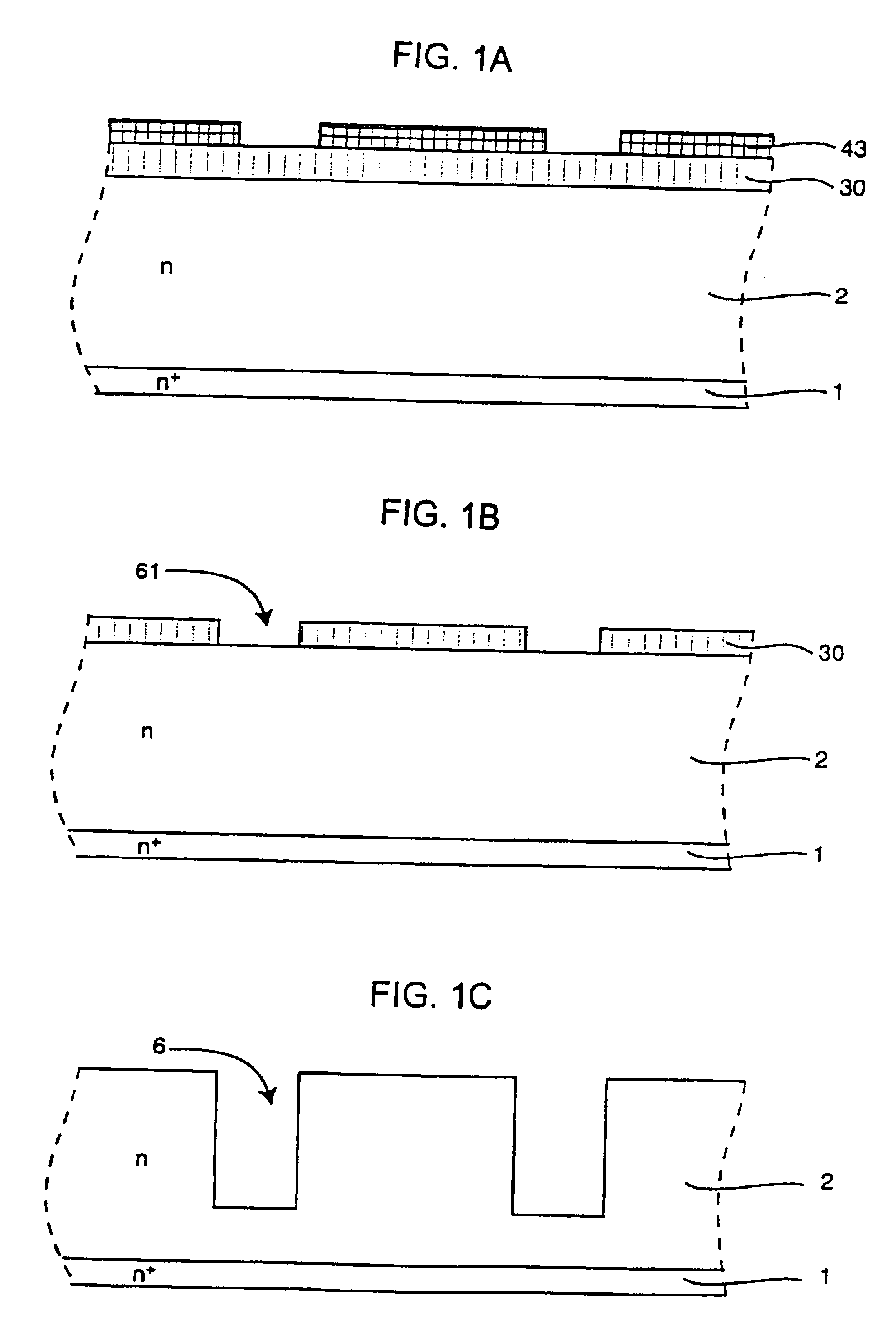
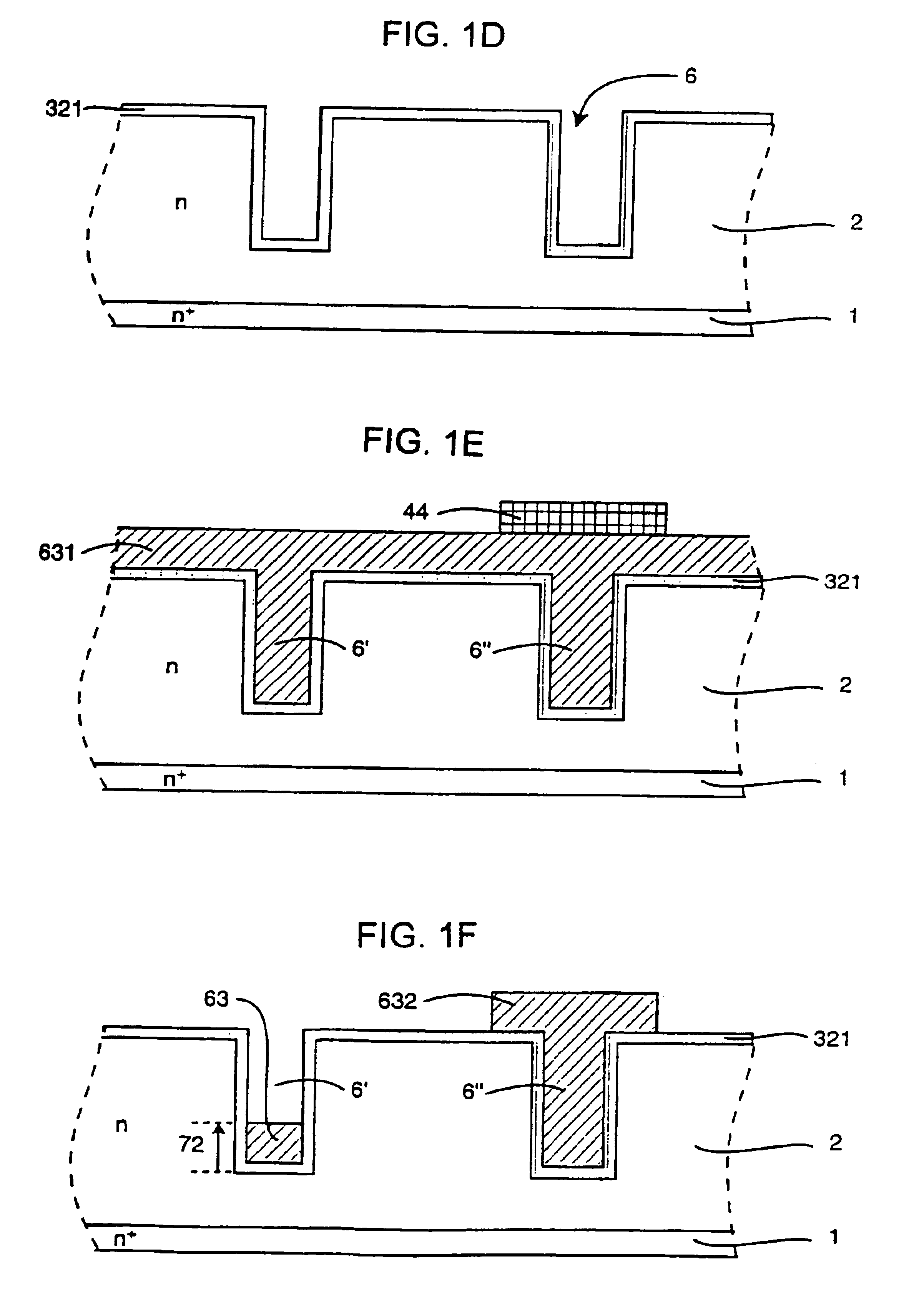
[0157]a) Provision of a highly doped n+-type substrate as starting material.[0158]b) Deposition of an n-type epitaxial layer with a dopant concentration of 1×1014 cm−3 to 1×1018 cm−3.[0159]c) Etching of the trenches using a patterned trench mask (oxide, TEOS 400 nm, photoresist). Removal of the trench mask. Fashioning of the trench as strip or as grid for a cell structure.[0160]d) Application of an insulation layer having a thickness of a few nm to a few μm. In this case, the insulation layer may[0161]also be a multilayer system (thermal oxide, deposited oxide, nitride)[0162]e) Deposition of a field electrode, in which case the material of the field electrode may contain doped polysilicon, silicides (tungsten silicide) and other conductive materials. In this case, a polysilicon is deposited with a layer thickness amounting to at least half the trench width, reduced by the thickness of the insulation layer.[0163]f) Masked or unmasked etching back of the field electrode to distinctly ...

example b

[0177]As example A, but after the etching back of the field electrode and a partial or complete removal of the first dielectric layer, the field electrode is etched back once more in order to reduce the gate-source capacitance. In this case, a nitride layer is optionally a constituent of the first dielectric layer. The nitride layer is patterned and, after the etching back of the field electrode, is utilized as an etching mask for etching the first dielectric layer.


PUM


Abstract

A method for fabricating a transistor configuration including at least one trench transistor cell has a gate electrode and a field electrode disposed in a trench below the gate electrode. The trenches are formed in a semiconductor substrate. A drift zone, a channel zone, and a source zone are in each case provided in the semiconductor substrate. According to the invention, the source zone and / or the channel zone are formed at the earliest after the introduction of the trenches into the semiconductor substrate by implantation and diffusion.

Description

BACKGROUND OF THE INVENTIONField of the Invention[0001]The present invention relates to a method for fabricating a transistor configuration including at least one trench transistor cell having a field electrode, in which at least one trench is introduced into a process layer of a semiconductor substrate, a field electrode and a gate electrode are provided in the trench in a manner electrically insulated in each case from one another and from the process layer, and at least in each case one drift zone, one channel zone, and one source zone are formed in the process layer.[0002]Present-day customary trench MOS power transistors (UMOSFET, u-shaped metal oxide semiconductor field effect transistor) are distinguished from older types of MOS power transistors (DMOSFET, double diffused MOSFET, VMOSFET, v-shaped MOSFET) by a very low on resistivity (rDS, on)[0003]In this case, the gate electrode of a trench transistor cell is disposed in a trench in the semiconductor substrate. The source a...

Claims


Application Information

Patent Timeline
Patent Type & Authority Patents(United States)
IPC IPC(8): H01L21/336H01L29/06H01L29/40H01L29/423H01L29/78
CPCH01L29/407H01L29/7813H01L29/7811H01L29/402H01L29/42368H01L29/4238H01L29/42376
Inventor HENNINGER, RALFHIRLER, FRANZKRUMREY, JOACHIMRIEGER, WALTERPOLZL, MARTINHOFER, HEIMO
Owner INFINEON TECH AG
Why Eureka
Try Eureka