

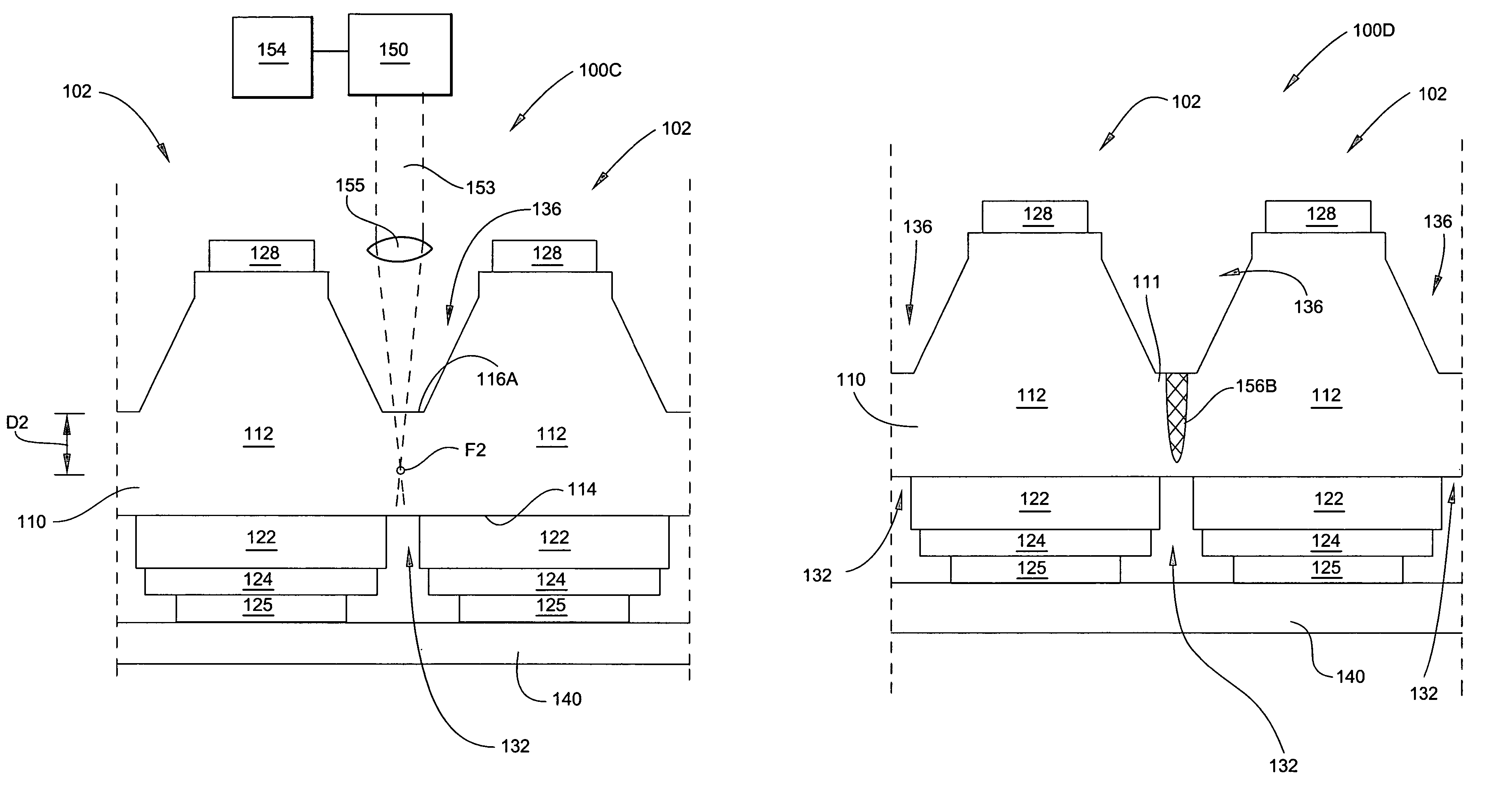
Semiconductor substrate assemblies and methods for preparing and dicing the same
a technology of semiconductor substrates and semiconductor devices, applied in the direction of manufacturing tools, metal working devices, welding/soldering/cutting articles, etc., can solve the problems of wafer breakage along the scribe line, individual semiconductor devices are typically extremely small compared to each other
- Summary
- Abstract
- Description
- Claims
- Application Information
AI Technical Summary
Benefits of technology
Problems solved by technology
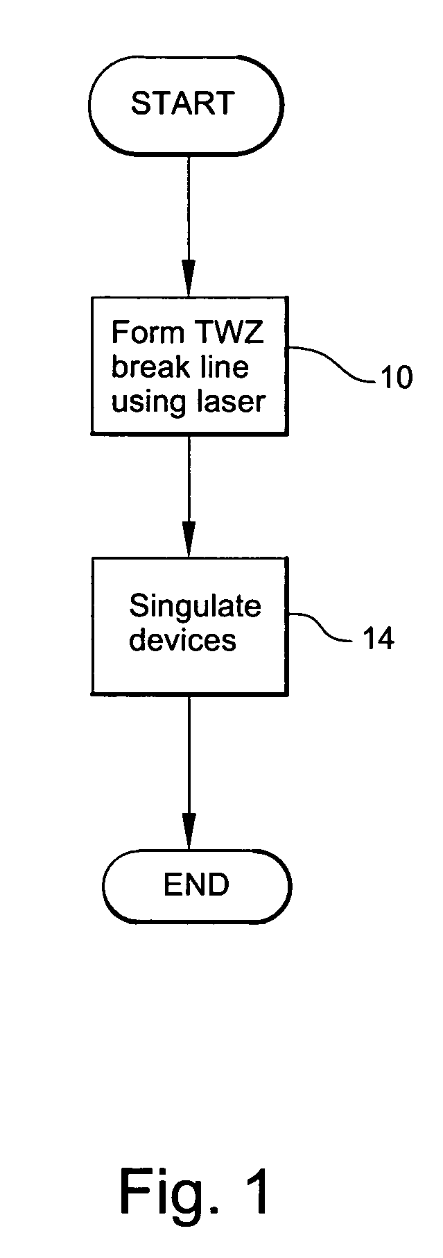
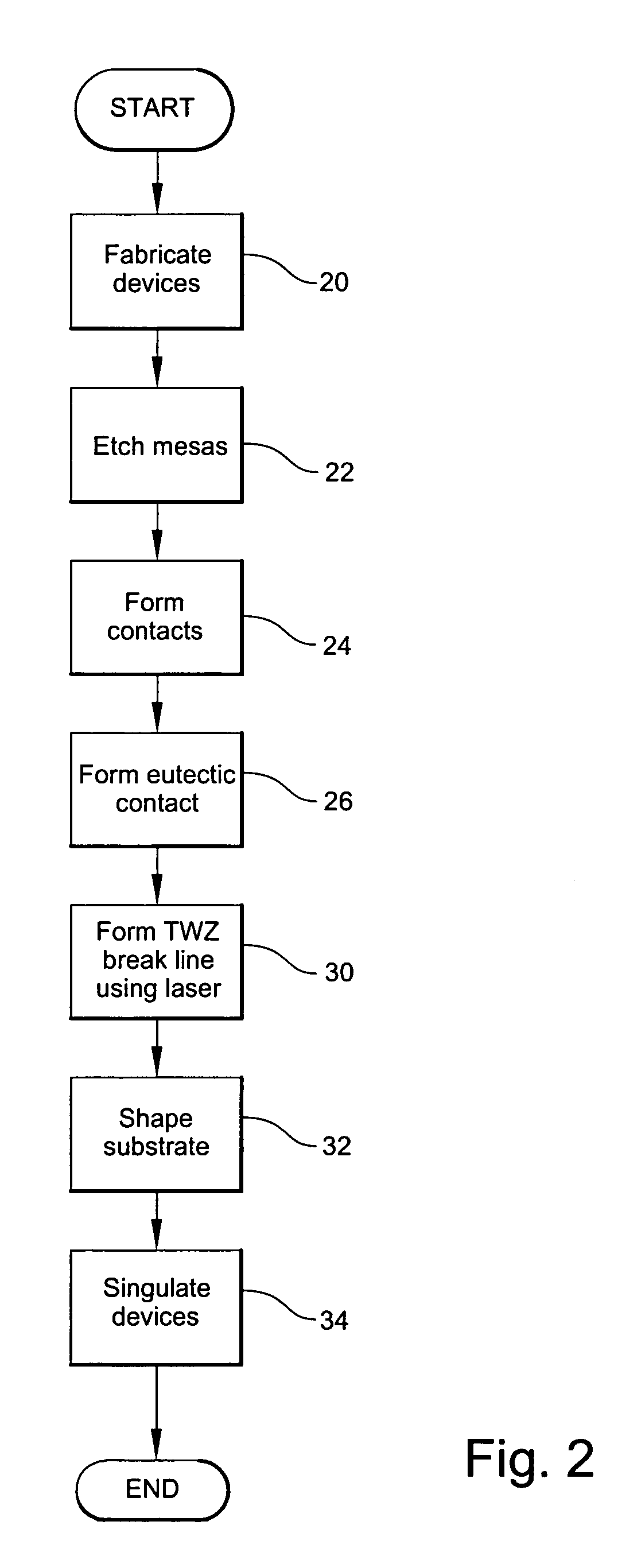
Method used
Image

Examples
example 1
[0070]FIGS. 12 and 13 are photographs of a first SiC wafer that was laser scribed with a depth of focus of the laser at the surface of the wafer. The wafer had a thickness of 250 μm. The wafer material was 6H SiC with a pitch pattern of 300 μm square dice. The wafer was sawn to form the inverted pyramid shape from the back side. The laser energy was applied to the mesa or epitaxy side of the wafer and directed in the center of the “streets” (i.e., the non-active portions between the dice). The wafer was thereafter broken along the scribe lines using a Dynatex break tool. The edge formed along a break is shown in FIGS. 12 and 13 at magnifications of 300× and 1000×, respectively. The break yield for the first wafer was approximately 85%.
example 2
[0071]FIGS. 14 and 15 are photographs of a second SiC wafer that was laser scribed with a depth of focus of the laser at 10 μm below the surface of the wafer. The wafer had a thickness of 250 μm. The wafer material was 6H SiC with a pitch pattern of 300 μm square dice. The wafer was sawn to form the inverted pyramid shape from the back side. The laser energy was applied to the mesa or epitaxy side of the wafer and directed in the center of the “streets.” The wafer was thereafter broken along the scribe lines using a Dynatex break tool. The edge formed along a break is shown in FIGS. 14 and 15 at magnifications of 300× and 1000×, respectively. Compared to the first wafer of Example 1, the second wafer of Example 2 has a more uniform and less rough break surface. The break yield for the second wafer was 100%.
PUM
| Property | Measurement | Unit |
|---|---|---|
| depth | aaaaa | aaaaa |
| width | aaaaa | aaaaa |
| depth | aaaaa | aaaaa |
Abstract
Description
Claims
Application Information