Surface treatment method and equipment

a surface treatment and equipment technology, applied in the field of objects and their manufacture, can solve the problems of physical and/or electrical damage to the surface being treated, charging and physical damage to the treatment chamber itself, and the difficulty of controlling conventional plasma processing techniques

Inactive Publication Date: 2006-03-21
MITZEL JIM +1
View PDF14 Cites 20 Cited by
  • Summary
  • Abstract
  • Description
  • Claims
  • Application Information

AI Technical Summary

Benefits of technology

[0007]According to the present invention, a technique including a method and apparatus for the manufacture of treating objects is provided. In an exemplary embodiment, the present invention provides a novel technique for treating a surface of an object using a plasma treatment apparatus.

Problems solved by technology

Conventional plasma processing techniques using hydrogen, however, often cause undesirable results.
For example, oxygen bearing plasmas often cause physical and / or electrical damage to surfaces being treated.
Additionally, higher high energy particles also cause charging and physical damage to the treatment chamber itself.
Conventional plasma processing techniques are also often difficult to control and may lead to plasma damage.

Method used


Image

  • Surface treatment method and equipment
  • Surface treatment method and equipment
  • Surface treatment method and equipment

Examples


examples

[0042]To prove the principle and operation of the present invention, examples have been provided. These examples are merely illustrations, which should not limit the scope of the claims herein. One of ordinary skill in the art would recognize many other variations, modifications, and alternatives. The present examples can be implemented using a tool such as the one in FIG. 7. The examples are as follows:

first example

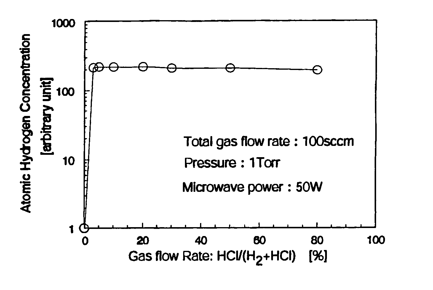
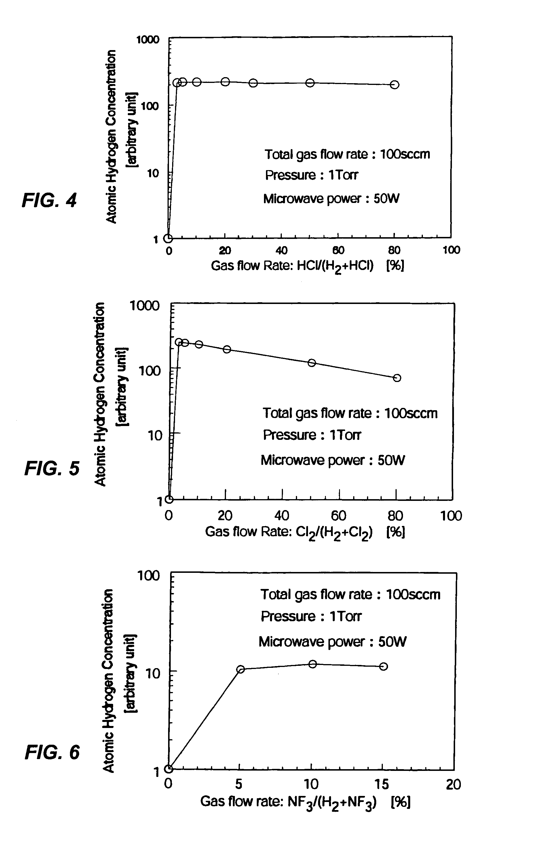
[0043]In the present example, the present method introduces gases (i.e., H2: 90 SCCM, Cl2: 10 SCCM) as a plasma source was activated in a tool similar to the one in FIG. 7. The plasma source was activated with 500 watt 2.45 GHz microwave, but can also be at other powers. An NF3 gas (at 100 SCCM) was added at a downstream area, while 6 inch Si wafer covered by silicon native oxide film mounted on a stage in the plasma tool. The silicon wafer surface was hydrophobic after plasma processing for 3 minutes at 2 Torr., which indicates that the silicon native oxide film was removed by this processing.

[0044]As well as the above, mixed gases (i.e., H2: 9 SCCM, HCl: 10 SCCM) as the plasma source gas was activated. The plasma was maintained at 500 watt 2.45 GHz microwave. An NF3 gas (at 100 SCCM) was added at a downstream area from the plasma source. A 6 inch Si wafer covered by silicon native oxide film was mounted on the stage in the plasma tool. The silicon wafer surface was hydrophobic aft...

second example

[0045]In the present example, mixed gases (i.e., H2: 90 SCCM, Cl2: 10 SCCM) are used as the plasma source gas in a tool similar to the one in FIG. 7. This source gas was activated with a power source including 500 watts at 2.45 GHz microwave energy. Silane (i.e., SiH4) gas (at 5 SCCM) was added at downstream area from the plasma processing region. A 6 inch Si wafer covered by silicon dioxide film was mounted on the stage in the plasma processing region, which was downstream from the plasma source. Then, the wafer temperature was elevated to 450° C. and maintained at such temperature. The processing pressure was pumped down to 2 Torr and also maintained at such pressure. In the present example, a deposited film was observed on the wafer surface after the processing the wafer for 1 hour. We believe that such film was a silicon film because the silicon wafer surface was completely hydrophobic just after the processing.


PUM

PropertyMeasurementUnit
dissociation ratioaaaaaaaaaa

Abstract

A method for treating material surface utilizing atomic hydrogen. The method includes utilizing atomic hydrogen by mixing halogen and/or halide to a gas which is used for generating, atomic hydrogen in the plasma. The present method also includes utilizing a characteristics of plasma downstream (11) in which the objective surface is prevented from physical damage caused by high energy particle and undesirable reactive species are controlled so as to avoid their influence. In an alternative embodiment, the present invention includes a method for a material surface treatment utilizing atomic hydrogen without the influence of atomic oxygen by using a gas, as a plasma source, containing the molecule and/or compound of chlorine, bromine and/or iodine and not containing molecules with oxygen atom.

Description

CROSS-REFERENCES TO RELATED APPLICATIONS[0001]This application claims priority to U.S. Ser. No. 60 / 088,739 filed Jun. 10, 1998, incorporated by reference herein.BACKGROUND OF THE INVENTION[0002]The present invention relates to objects and their manufacture. More particularly, the invention is illustrated in an example using a novel combination of gases and a downstream plasma surface for selectively treating surfaces for substrates used in semiconductor integrated circuits. Merely by way of example, the invention can be applied in the manufacture of other substrates such as flat panel displays, micro electrical mechanical machines (“MEMS”), sensors, optical devices, and others.[0003]In the manufacture of objects such as integrated circuits, processing safety and reliability have been quite important. Fabrication of integrated circuits generally requires numerous processing steps such as etching, deposition, photolithography, and others. In the manufacture of semiconductor wafers, th...

Claims


Application Information

Patent Timeline
Patent Type & Authority Patents(United States)
IPC IPC(8): H01L21/00
CPCC23G5/00H01L21/02046H01J37/32357H01J37/32192
Inventor FUJIMURA, SHUZOTAKAMATSU, TOSHIYUKI
Owner MITZEL JIM
Why Eureka
Try Eureka