Method for optimizing inspection speed in low, and fluorescent light applications without sacrificing signal to noise ratio, resolution, or focus quality

a low-speed, fluorescent light technology, applied in the direction of instruments, television systems, optical elements, etc., can solve the problems of not being cost effective or practical to increase the size of the laser, not being feasible, practical or cost-effective to increase the illumination power, and the life of the bulb also becoming an issue in high-power illumination systems, so as to increase the life of the bulb, reduce the intensity of illumination, and increase the effect of camera signal

Inactive Publication Date: 2006-03-21
BELTRONICS
View PDF6 Cites 51 Cited by
  • Summary
  • Abstract
  • Description
  • Claims
  • Application Information

AI Technical Summary

Benefits of technology

[0018]illumination intensity is reduced to increase bulb life.
[0019]The camera signal can be greatly increased by increasing the numerical aperture (NA) of the imaging optics. Equation 7 states that camera signal strength is proportional to NA2. However, the optical depth of focus (DOF) given by the equation:
[0020]Table 1 is a list of commercially available lenses from the Zeiss Corporation. The table lists the depth of focus, numerical aperture, resolving power, light collection coefficient, light collection cone angle, working distance magnification and part number for each lens.
[0021]TABLE 1Commercially Available Objective Lenses From ZeissResolvingDepth ofPower forFocusLightLight Collectionλ = 0.55λ = 0.55Magnification / NumericalCollectionCone Angle(Microns)(Microns)Workingpixel size(microns)Zeiss PartNumberAperture(NA)Coefficient(NA2)(degrees)θ = 2 × sin3(NA)λ2×NAλ2×NA2Distance(WD)1.25× / 10.44423000.0350.00124.07.82293.9 mm2.5× / 5.24423100.0750.00568.63.6499.4 mm5× / 2.64403200.150.0225171.812.213.6 mm 5× / 2.6—0.250.0625291.14.4—10× / 1.34428320.250.0625291.14.412.7 mm 10× / 1.34423300.300.0900350.93.15.7 mm20× / 0.654428400.400.1600470.71.79.8 mm10× / 1.34401350.500.2500600.51.12.0 mm20× / 0.654423400.500.2500600.51.11.4 mm
[0022]Note that in Table 1 the 1.25X lens with an NA of 0.035 has a depth of focus of 229 microns whereas the 20X lens with an NA of 0.50 only has a depth of focus of 1.1 microns. However, for a through the lens illumination system as shown in FIG. 2, the 20X 0.5 NA lens collects 204 times (0.5 / 0.035)2 more light than the 1.25X 0.035 NA lens. Unfortunately, unless focus can be maintained to within the 1.1 micron depth of focus, the 20X 0.5 NA lens cannot be used to inspect the part. With current wafers 300 mm in diameter (300,000 microns) and circuit boards or flat panel displays over 700 mm (700,000 microns), maintaining focus to within microns becomes very difficult. Therefore, many inspection systems are forced to use low NA optics, which limits their ability to inspect low reflectivity and fluorescent parts at high speeds. As another example, consider the 5X 0.15 NA and the 5×0.25 NA lens, both with the same magnification. The 0.25 NA lens collects 2.7 times more light than the 0.015 NA lens, but only has a depth of field of 4.4 microns as compared to 12.2 microns. While the 0.25 NA lens enables the system to operate 2.7 times faster than the 0.15 NA lens, this lens can only be used if focus can be maintained to within 4 microns.
[0023]Another advantage of high NA optics is higher resolution. Resolving power is given by the equation: Resolving⁢⁢power=λ2×NAEquation⁢⁢11

Problems solved by technology

However, in low camera light conditions, which occur in most fluorescent inspection applications or for inspection of low reflectivity parts, both of which correspond to small values of Ref in Equation 7, it may not be feasible, practical, or cost effective to increase illumination power.
Fluorescent inspection systems, such as the Orbotech Blazer or Beltronics Mscan III, use expensive lasers as the illumination source.
In such systems, it is not cost effective or practical to increase the size of the laser.
In extremely fast non-fluorescent scan applications, bulb life also becomes an issue for high power illumination systems.
Therefore, inspection systems in which camera light is limited because:fluorescence is used to image the part,material reflectivity is low, andillumination intensity is reduced to increase bulb life.
Therefore, if signal strength is increased by using higher NA optics, it may not be possible to maintain focus as the part is scanned. FIG. 1 in the drawings shows the depth of focus ray diagram for a low S1 and high S2 NA lens.
Unfortunately, unless focus can be maintained to within the 1.1 micron depth of focus, the 20X 0.5 NA lens cannot be used to inspect the part.
With current wafers 300 mm in diameter (300,000 microns) and circuit boards or flat panel displays over 700 mm (700,000 microns), maintaining focus to within microns becomes very difficult.
Therefore, many inspection systems are forced to use low NA optics, which limits their ability to inspect low reflectivity and fluorescent parts at high speeds.
However, high NA optics cannot be used unless focus can be maintained as the part is scanned.
Therefore, many inspection systems, which do not have auto focus capability, are forced to use low NA optics to maintain focus and are unable to inspect very small features that require high magnification and high resolution.
However, these systems are not suited for high-speed inspection applications because they are slow, with focus time being proportional to the size and flatness of the part.
However, this method is not applicable for inspection of smooth homogeneous materials such as circuit board and wafer substrates and resists, which do not contain significant grain, texture, or high frequency information.
This technique has two major limitations When the magnification is high corresponding to a small field of view (FOV), small variations in focus height project the slits totally out of the FOV leaving nothing to focus on, as shown in FIG. 4.
When the slits are projected out of the FOV, the time required to find optimal focus greatly increases because. the focus algorithm cannot determine in which direction to move.
As a result of this hunting, the algorithm is easily confused and can become very slow.
This drastically increases the time required to compute the entire focus map such that this computation may take more time than the actual inspection process, which occurs immediately after the map has been calculated.

Method used


Image

  • Method for optimizing inspection speed in low, and fluorescent light applications without sacrificing signal to noise ratio, resolution, or focus quality
  • Method for optimizing inspection speed in low, and fluorescent light applications without sacrificing signal to noise ratio, resolution, or focus quality
  • Method for optimizing inspection speed in low, and fluorescent light applications without sacrificing signal to noise ratio, resolution, or focus quality

Examples


Embodiment Construction

1. Focus by Minimizing Width of Target

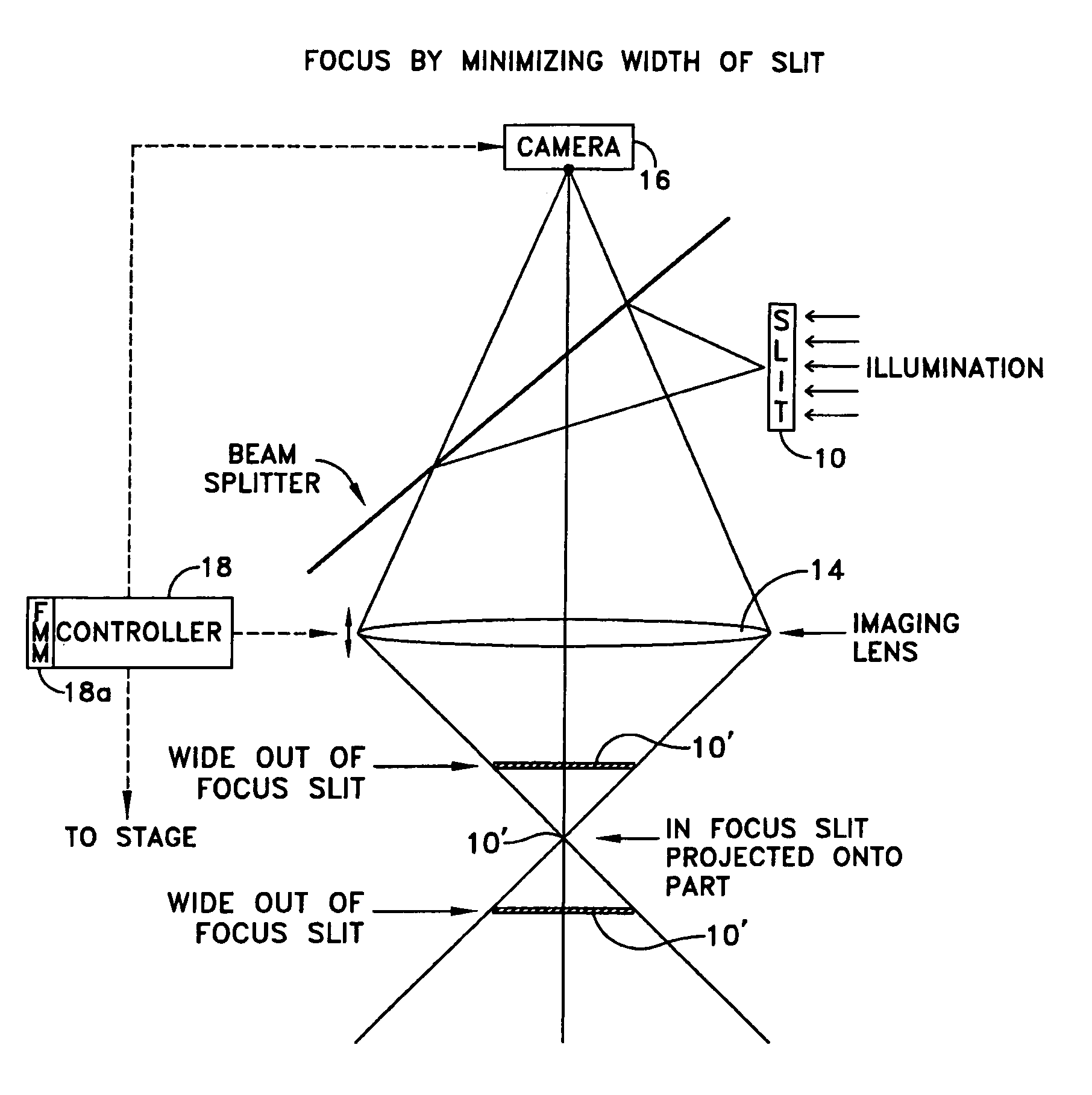
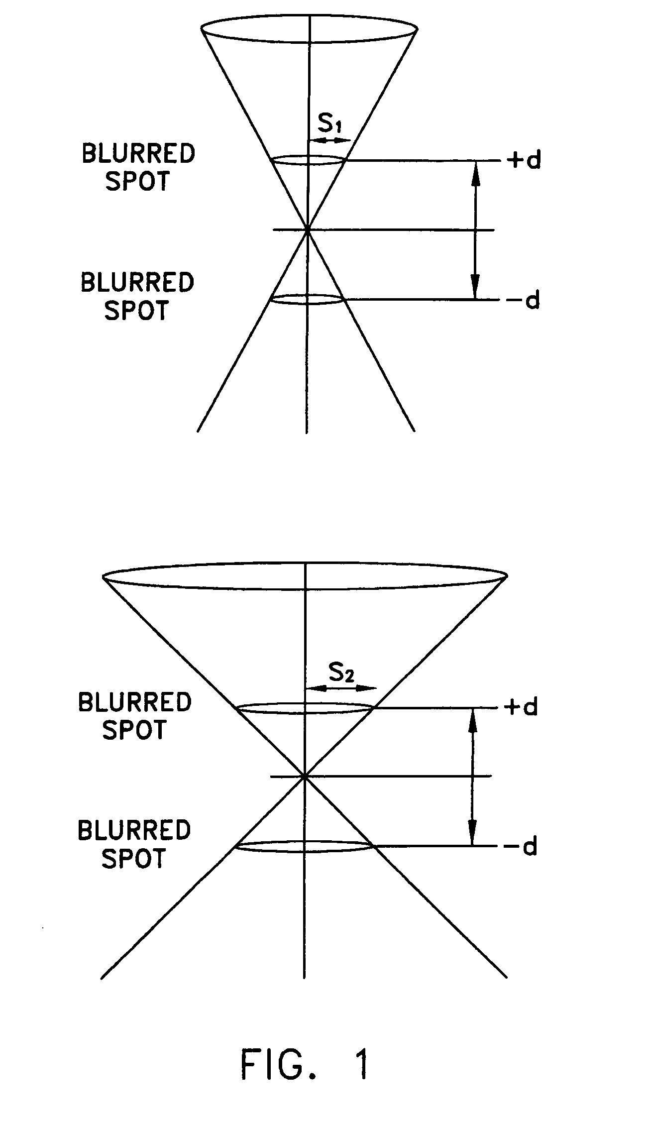
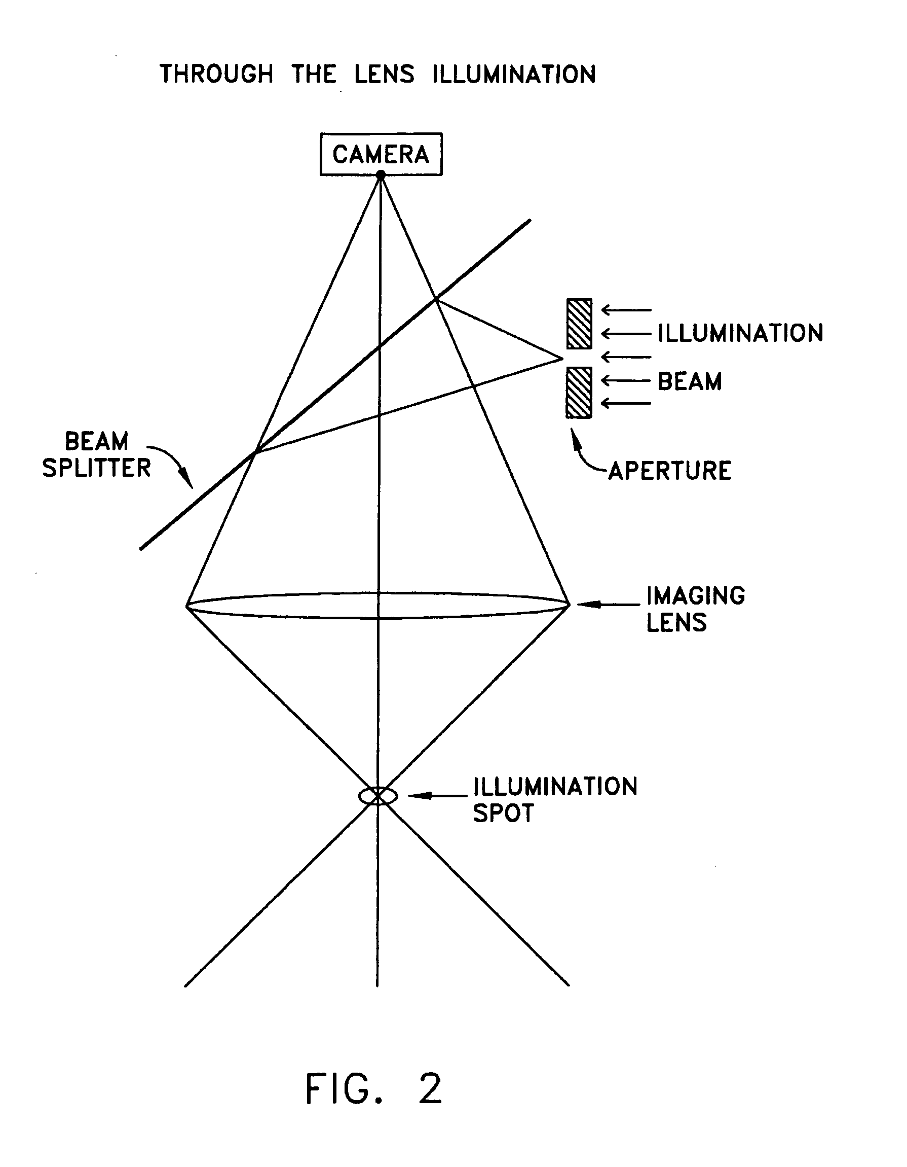
[0056]Referring to FIG. 5, in accordance with this method, a target 10 in the form of a slit is projected by way of a beam splitter 12 through the imaging lens 14 of an inspection camera 16 onto a part or workpiece supported by a scanning stage (not shown). While the illustrated target is a slit, it could just as well be a small dot or an edge. In any event, at all positions along the Z-axis, light from the target 10 is present as shown by the target images 10′. As seen in FIG. 5, when the imaging optics are out of focus in the Z direction, the target image 10′ is relatively wide. On the other hand when those optics are in focus, the image 10′ has minimum width. Light from the part including the target image is reflected back through lens 14 and the beam splitter 12 to camera 16 which is preferably a CCD camera (see my U.S. Pat. Nos. 5,119,434 and 4,697,088) with high NA (0.05 or larger) optics. Thus, unlike the prior system described above in c...


PUM

PropertyMeasurementUnit
depth of focusaaaaaaaaaa

Abstract

The method for optimizing inspection speed during optical inspection of parts in high, low and fluorescent light applications. There are described autofocus mechanisms and methods optimized for fluorescent and non-fluorescent applications that when combined with a high speed CCD camera and high numerical aperture (NA) optics, achieve superior signal to noise ratio, resolution, and inspection speed performance.

Description

CROSS-REFERENCE TO RELATED APPLICATION[0001]This application claims the benefit of Provisional Application No. 60 / 433,817 filed Dec. 16, 2002.BACKGROUND OF THE INVENTION[0002]Inspection of electronic parts such as such as wafers, circuit boards, flat panel displays, multi-chip modules, and high-density electronic packages requires sufficient camera signal to noise ratio (S / N) to image the part, a fast camera clock rate to obtain good throughput, and sharp focus with high resolution to insure detection of small defects.[0003]Camera signal output is given by the equation: Camsig=⁢Illumination⁢⁢Power#⁢⁢cam⁢⁢pixels×OE×⁢Ref×Integration⁢⁢time×NA2Equation⁢⁢1where:[0004]Illumination Power=total illumination power incident on the part[0005]OE=efficiency or transmittance of the optical system Integration time=time duration over which light is collected by the camera[0006]# cam pixels=the total number of camera pixels[0007]NA2=the numerical aperture of the imaging optics[0008]Ref=the percent o...

Claims


Application Information

Patent Timeline
Patent Type & Authority Patents(United States)
IPC IPC(8): G02B27/64G01N21/88G01N21/956G02B7/30G02B7/32
CPCG01N21/8806G02B7/32G01N21/956G02B7/30G01N21/88
Inventor BISHOP, ROBERT
Owner BELTRONICS
Why Eureka
Try Eureka