Electron beam processing method

a processing method and electron beam technology, applied in the direction of vacuum evaporation coating, solid-state diffusion coating, coating, etc., can solve the problems of lowering processing accuracy, difficult to adapt to material that requires processing without, damage in scanning range, etc., to achieve high resolution, easy to detect the position of a formed film, good accuracy

Active Publication Date: 2006-03-28
HITACHI HIGH TECH SCI CORP
View PDF3 Cites 27 Cited by
  • Summary
  • Abstract
  • Description
  • Claims
  • Application Information

AI Technical Summary

Benefits of technology

[0009]If a material having a material contrast difference of at least a few percent from the material to be processed, in a secondary electron image, is formed by electron beam CVD in the vicinity of the region to be processed, since it is possible to easily detect the position of a formed film, even with a thin film, from this quality contrast difference, processing is carried out with drift correction during processing using the same method as for the projection described above. If this method is used, it is possible to make a marker for drift correction in a shorter time than in the case of the projection described above.
[0010]Naturally, calculation of drift amount for correcting the electron beam irradiation region at the time of processing does not have to compare position of a spot marker, and it is possible to form a characteristic microscopic pattern that can measure displacement in an X direction and a Y direction, such as a cross, instead of the spot marker, and to obtain the drift amount from pattern matching of a secondary electron image containing the characteristic microscopic pattern.
[0011]Since drift is corrected using an image obtained by scanning with an electron beam, there is no damage to a microscopic CVD film or the periphery thereof as there is with an ion beam. Because a deposition film is used as a marker for drift correction, there are no problems such as filling in of holes of a drift correction marker or dropping of accuracy due to holes being large, as with the related art technology. Also, since drift amount of a microscopic projection is obtained, drift correction can be carried out with high precision.

Problems solved by technology

However, with a focused ion beam device, since the extent of damage to a processed region having high film formation and etching rates due to ion beam injection is large, it is difficult to adapt to material that requires processing without damage, and for this type of material there is a demand for processing of microscopic regions using electron beam processing that causes hardly any damage.
Also, with a focused ion beam processing device, when carrying out drift correction such as described above, as well as the processing region, there is also damage in a scanning range used for the drift correction, and depending on the situation there may also be removal of material due to physical sputter effect.
Also, if holes formed by an ion beam for drift correction are too small, the holes may be filled in during film deposition and etching making drift correction impossible and lowering processing accuracy, while if the holes formed are too large the holes cause lowering of processing quality.

Method used


Image

  • Electron beam processing method
  • Electron beam processing method
  • Electron beam processing method

Examples


Embodiment Construction

[0015]An example of the present invention adopted in photomask defect correction will be described in the following.

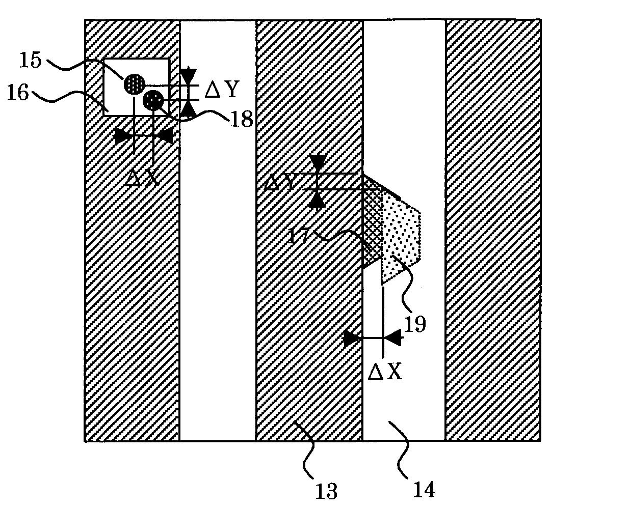
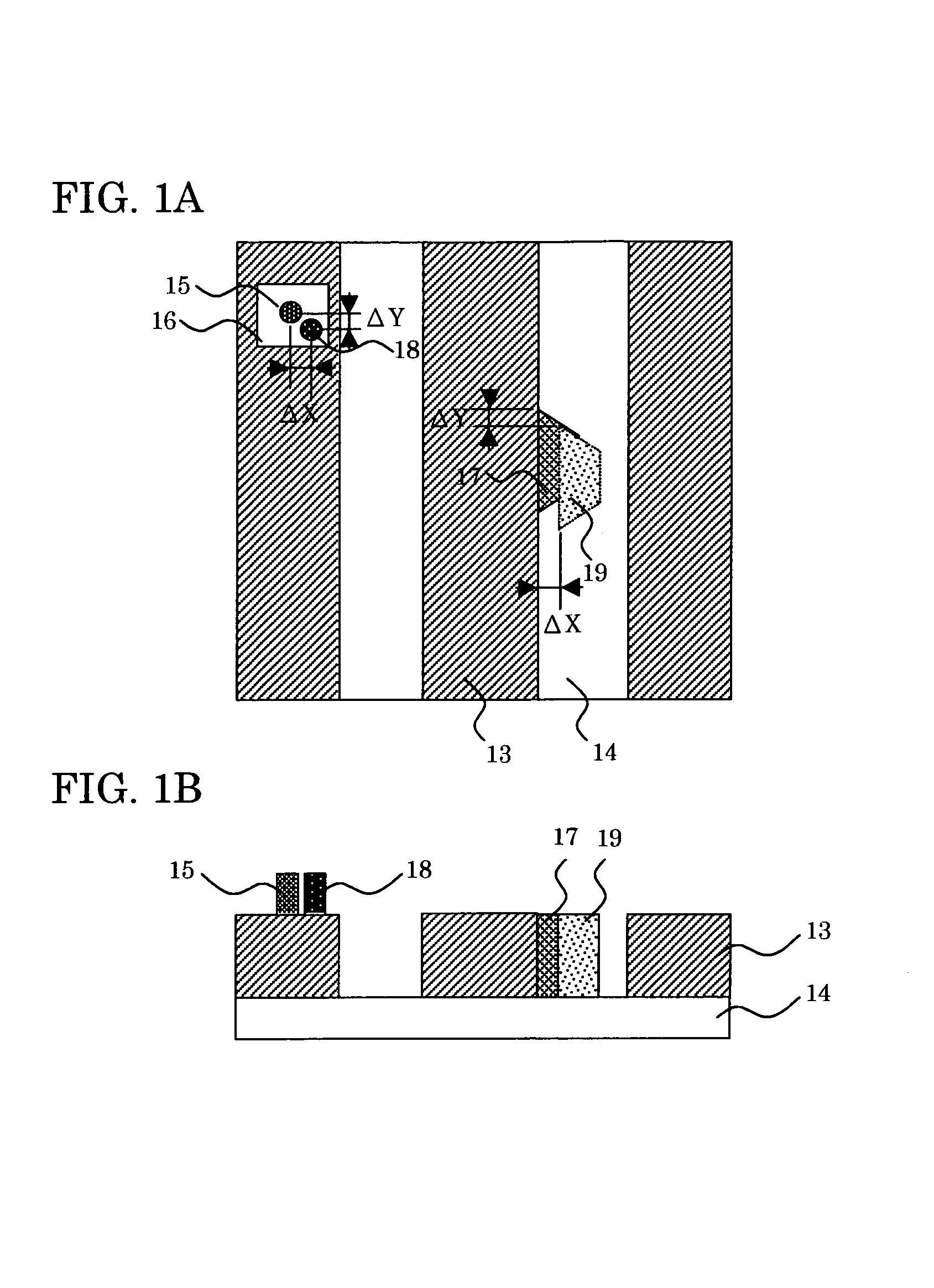
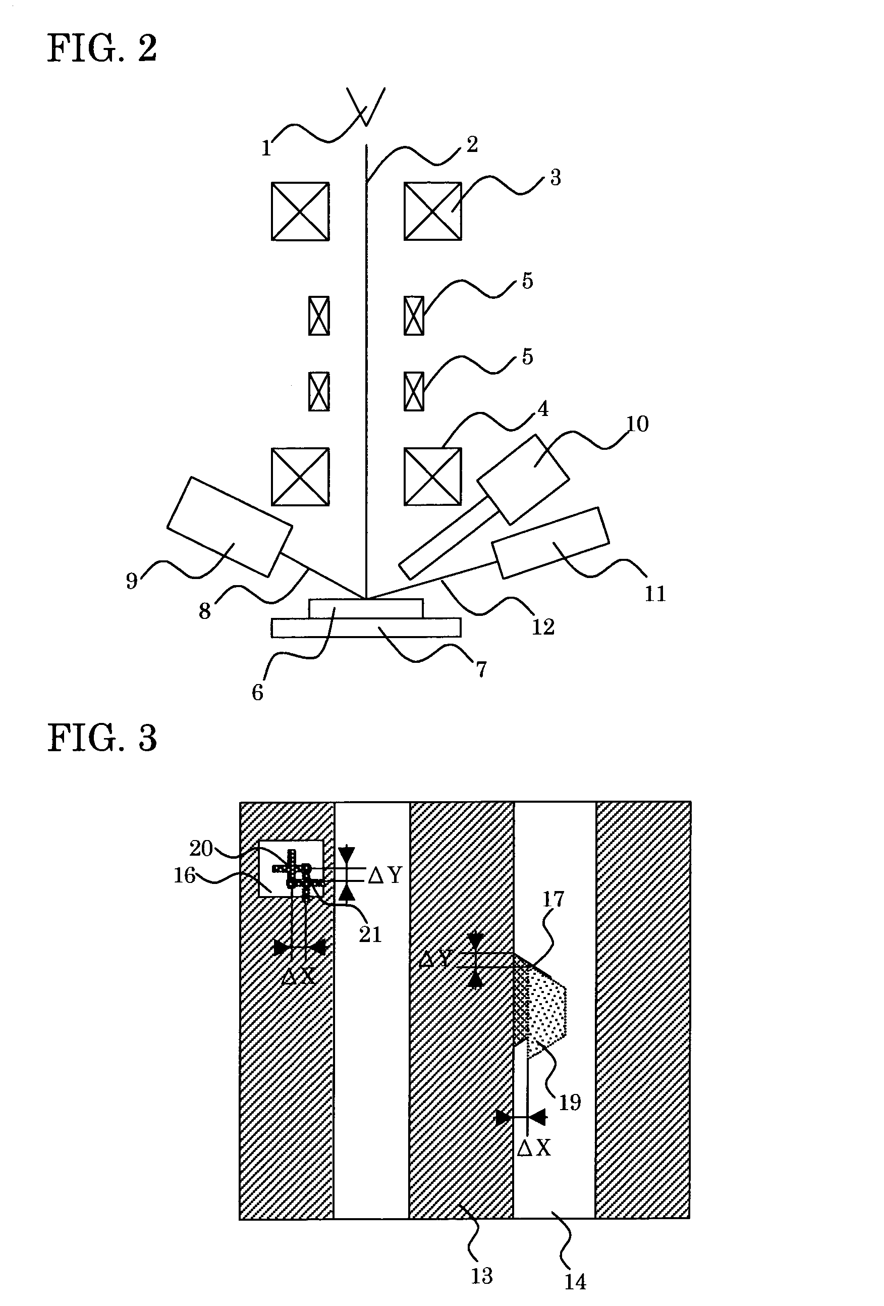
[0016]A sample in the form of a photomask 6 (binary mask or phase shift mask) containing defects is brought into a vacuum chamber of an electron beam device provided with a mechanism for introducing masking film source material gas or etching assist gas, as shown in FIG. 2, and an XY stage 7 is moved to defect positions detected by a defect inspection device. First of all, an electron beam 2 ejected from the field emission electron source (so called electron gun) 1 and accelerated to 500V–3 kV is focused by an electromagnetic condenser lens 3 and an electromagnetic objective lens 4, secondary electrons 8 generated when the electron beam 2 is scan-irradiated on the photomask 6 by an electromagnetic deflector 5 are captured by a secondary electron detector 9 in synchronism with the scanning period, the place where a microscopic projection is formed is determined from a s...


PUM

PropertyMeasurementUnit
sizeaaaaaaaaaa
displacementaaaaaaaaaa
shapeaaaaaaaaaa

Abstract

A microscopic projection or a characteristic pattern are formed in the vicinity of a region to be processed before processing using electron beam CVD, during processing an image of a region containing the projection or pattern formed by electron beam CVD is captured to obtain a current position of the projection or pattern, a difference between the position before staring and the current position is treated as a drift amount and processing is restarted at a region that has been subjected to microscopic adjustment of the electron irradiation region.

Description

BACKGROUND OF THE INVENTION[0001]The present invention relates to high precision processing technology for a processing device for a microscopic region using an electron beam.[0002]With respect to demands for high precision processing of microscopic regions of local domains that has increased in recent years, exemplified by semiconductor fine processing, magnetic storage devices and MEMS, since with an electron beam device such as a scanning electron microscope or a transmission electron microscope film deposition rate and etching rate are lowered even while indicating capability due to high image resolution, up to now focused ion beam devices having high film formation and etching rates have been used in high precision processing of microscopic regions.[0003]However, with a focused ion beam device, since the extent of damage to a processed region having high film formation and etching rates due to ion beam injection is large, it is difficult to adapt to material that requires proce...

Claims


Application Information

Patent Timeline
Patent Type & Authority Patents(United States)
IPC IPC(8): C23C16/00C23C16/48C23C16/52
CPCC23C16/52C23C16/486
Inventor TAKAOKA, OSAMUHAGIWARA, RYOJI
Owner HITACHI HIGH TECH SCI CORP
Why Eureka
Try Eureka