Polishing pad surface condition evaluation method and an apparatus thereof and a method of producing a semiconductor device

a technology of condition evaluation and polishing pad, which is applied in the direction of abrasive surface conditioning devices, lapping machines, instruments, etc., can solve the problems of lithography, which is indispensable for forming wiring, and the unevenness of the wafer surface has increased,

Inactive Publication Date: 2006-03-28
HITACHI LTD
View PDF5 Cites 34 Cited by
  • Summary
  • Abstract
  • Description
  • Claims
  • Application Information

AI Technical Summary

Benefits of technology

[0018]The embodiments of the present invention eliminate the problems of the conventional technology described above and provide a method for evaluating polishing pad surface conditions that directly evaluates the polishing pad surface conditions, a device for the same, and a method for producing thin-film devices using the same.

Problems solved by technology

As a result, unevenness of a wafer surface has increased.
Such unevenness of a wafer surface makes lithography, which is indispensable for forming wiring patterns and the like, difficult.
An important issue in CMP processing is the management of pad surface conditions used in the polishing process.
However, no effective method for performing direct evaluation has been established.
In CMP processing, if a single pad is used to polish a large number of wafers, the pad will deteriorate and the polishing rate will decrease.
This reduction of polishing rate results from the fact that the planarity of the pad surface increases as wafers are polished.
This deterioration does not occur uniformly on the pad surface.
With this type of indirect method, the pad surface conditions cannot be accurately evaluated.
Also, evaluation requires time and cannot be performed in response to sudden problems, thus resulting in many defects.
Also, when a single pad has been used for a certain amount of processing, the polishing rate of the pad will not be restored even when conditioning is performed.
However, indirect evaluation based on polishing rates will not provide an accurate evaluation of pad surface conditions and there are variations in the polishing rates themselves.
Thus, the pad life span cannot be accurately evaluated, resulting in pads being replaced before their life span is reached.

Method used


Image

  • Polishing pad surface condition evaluation method and an apparatus thereof and a method of producing a semiconductor device
  • Polishing pad surface condition evaluation method and an apparatus thereof and a method of producing a semiconductor device
  • Polishing pad surface condition evaluation method and an apparatus thereof and a method of producing a semiconductor device

Examples


Embodiment Construction

[0049]The following is a description of specific embodiments of the present invention.

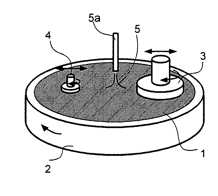
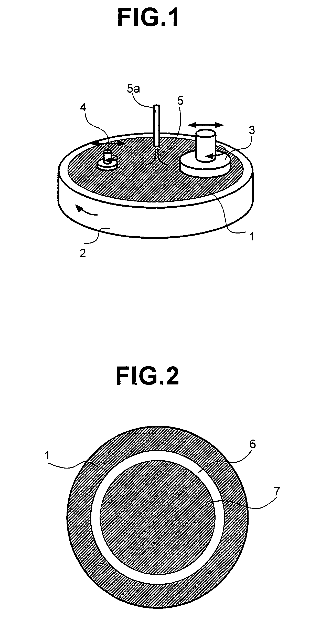
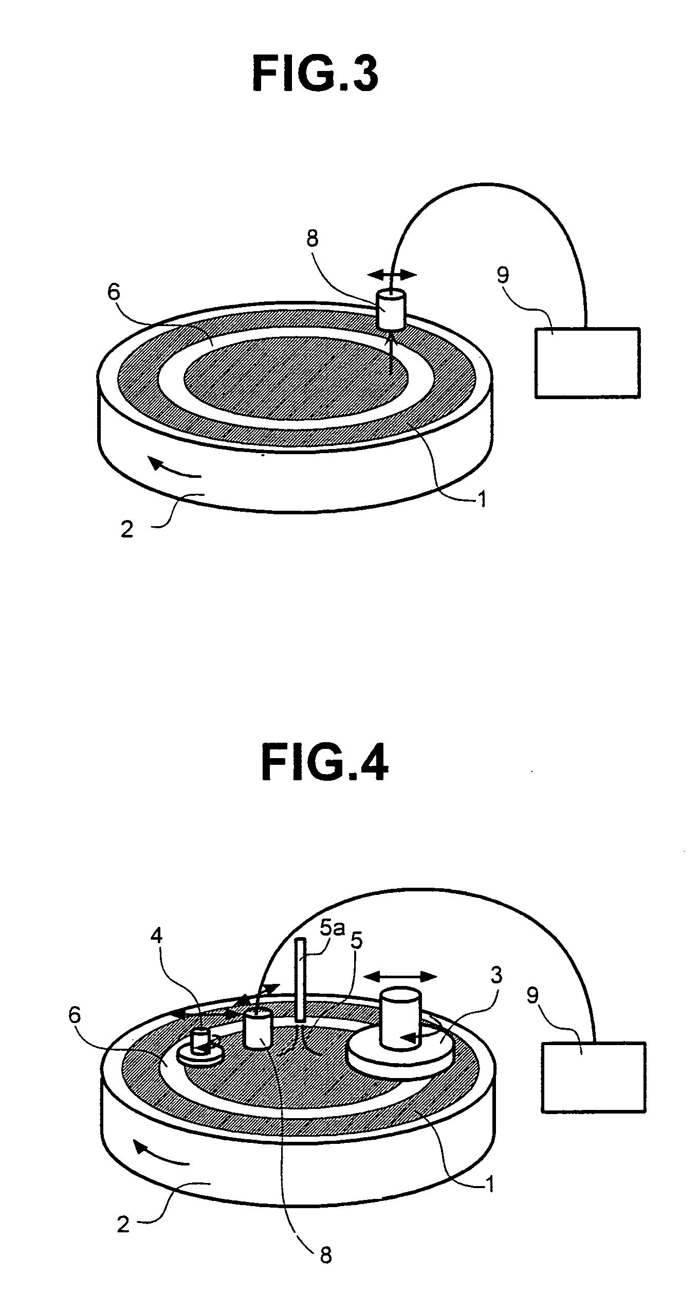
[0050]This description will use as an example a polishing process in which the item to be polished is a thin film with an uneven surface is formed on a substrate, and a polishing pad is used to polish the surface and make it planarized. An illumination light source is selected according to the structure of a detection optical surface, e.g., a monochromatic light such as a laser light source or a white light such as a halogen lamp.

[0051]First, six representative examples of how the surface condition of the polishing pad is evaluated will be described.

[0052](1) During the polishing process, a light such as a monochromatic laser light is used to illuminate the surface of the polishing pad. The light reflected from the illuminated region of the polishing pad is detected using an optical system. The surface condition of the polishing pad is evaluated based on the detected intensity of the reflected ligh...


PUM

PropertyMeasurementUnit
surface conditionsaaaaaaaaaa
areaaaaaaaaaaa
optical imagingaaaaaaaaaa

Abstract

The object of the present invention is to establish a technology for directly evaluating polishing pad surface conditions, to allow high-precision CMP process management, and to improve process throughput. The pad surface is illuminated with light. The intensity of reflected light or fluorescence from the illuminated area or an intensity distribution image is used directly evaluate the pad surface condition. Based on the results of this evaluation, conditioning conditions for a conditioner are optimized, thus allowing high-precision CMP processing while maintaining good pad surface conditions.

Description

BACKGROUND OF THE INVENTION[0001]The present invention relates to a method for evaluating polishing pad surface conditions, a device for the same, and a method for producing thin film devices using the same.[0002]Polishing pads are commonly used in the polishing process of production lines for various electronic parts. A method used in semiconductor device production lines, in which a surface is polished to be plane through chemical and mechanical operations (CMP: Chemical Mechanical Polishing), will be described below as a representative example of a polishing process.[0003]Semiconductor devices are produced by forming devices and wiring patterns on a silicon wafer through deposition, lithography, etching, and the like. In recent years, there has been a growing trend toward miniaturization and multi-layering to provide higher precision and higher densities in devices.[0004]As a result, unevenness of a wafer surface has increased. Such unevenness of a wafer surface makes lithography...

Claims


Application Information

Patent Timeline
Patent Type & Authority Patents(United States)
IPC IPC(8): G06K9/00G01B11/30B24B37/00B24B37/11B24B37/20B24B37/24B24B49/12B24B53/00B24B53/017G01N21/41H01L21/304
CPCB24B37/20G01N21/55B24B49/12G01N21/41
Inventor HIROSE, TAKENORIKOJIMA, HIROYUKINOMOTO, MINEOAIUCHI, SUSUMU
Owner HITACHI LTD
Why Eureka
Try Eureka