Permanent light coupling arrangement and method for use with thin silicon optical waveguides

a technology of optical waveguides and coupling arrangements, which is applied in the direction of optics, instruments, optical light guides, etc., can solve the problems of inability to realize the full set of specifications of the component in the integration platform, the material cost of silicon-based devices is considerably lower than, and the method of fabricating the component is not compatible, so as to facilitate the attachment of the prism coupler, and improve the coupling efficiency

Active Publication Date: 2006-03-28
CISCO TECH INC
View PDF6 Cites 34 Cited by
  • Summary
  • Abstract
  • Description
  • Claims
  • Application Information

AI Technical Summary

Benefits of technology

[0016]In order to provide optical coupling in accordance with the present invention, the silicon waveguide is doped to exhibit a refractive index that is slightly less than the prism coupler (refractive index of silicon≈3.5). An intermediate evanescent coupling layer, disposed between the waveguide and the prism coupler, is formed of a material with a refractive index less than both the prism and the waveguide. In one embodiment, the evanescent coupling layer comprises a constant thickness. In an alternative embodiment, the thickness of the evanescent coupling layer changes monotonically (along the direction of propagation in the waveguide) to improve the coupling efficiency between the prism and the waveguide. For the purposes of the present discussion, such an evanescent coupling layer will hereinafter be referred to as a “tapered” evanescent coupling layer.
[0017]In various embodiments of the pre

Problems solved by technology

Multi-module optoelectronic integration is required when a desired component is incompatible with the integrated device.
In some cases, no method of fabricating the component is compatible with the technology being considered, while in others it may be impossible to realize the full set of specifications for the component in the integration platform.
In addition, the material costs of silicon-based devices are considerably lower than those for competing technologies such as gallium arsenide or indium phosphide.
However, since silicon-based lasers are just beginning to be developed, it is not currently possible to incorporate the light source in the same silicon wafer as the signal processing and receiver elements.
Therefore, it is clear that this edge coupling technique is not readily applicable for use with relatively thin, sub-micron single mode silicon waveguides.
As direct coupling in the above-described manner does not provide a sufficiently small spot size, alternative techniques to transfer light into the waveguide must be used.
While coupling light into and out of a thin waveguide by launching light into and retrieving light from a high-index prism or prisms in close proximity to th

Method used


Image

  • Permanent light coupling arrangement and method for use with thin silicon optical waveguides
  • Permanent light coupling arrangement and method for use with thin silicon optical waveguides
  • Permanent light coupling arrangement and method for use with thin silicon optical waveguides

Examples


Embodiment Construction

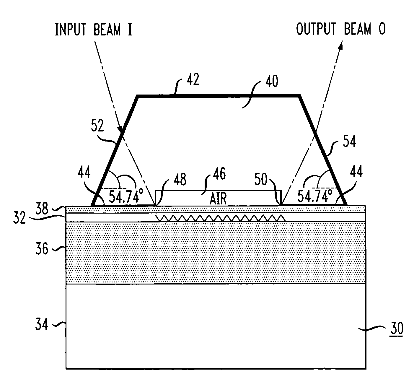
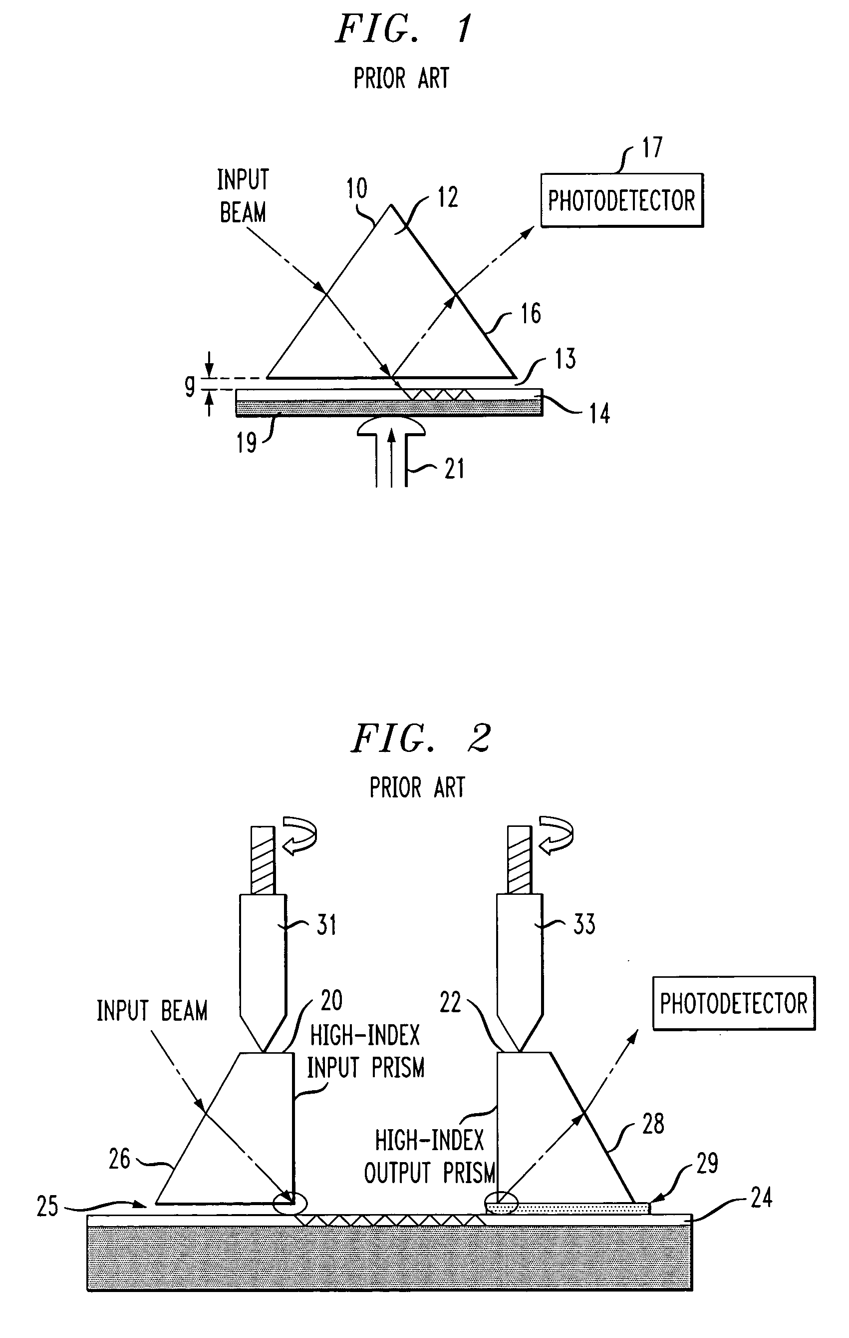
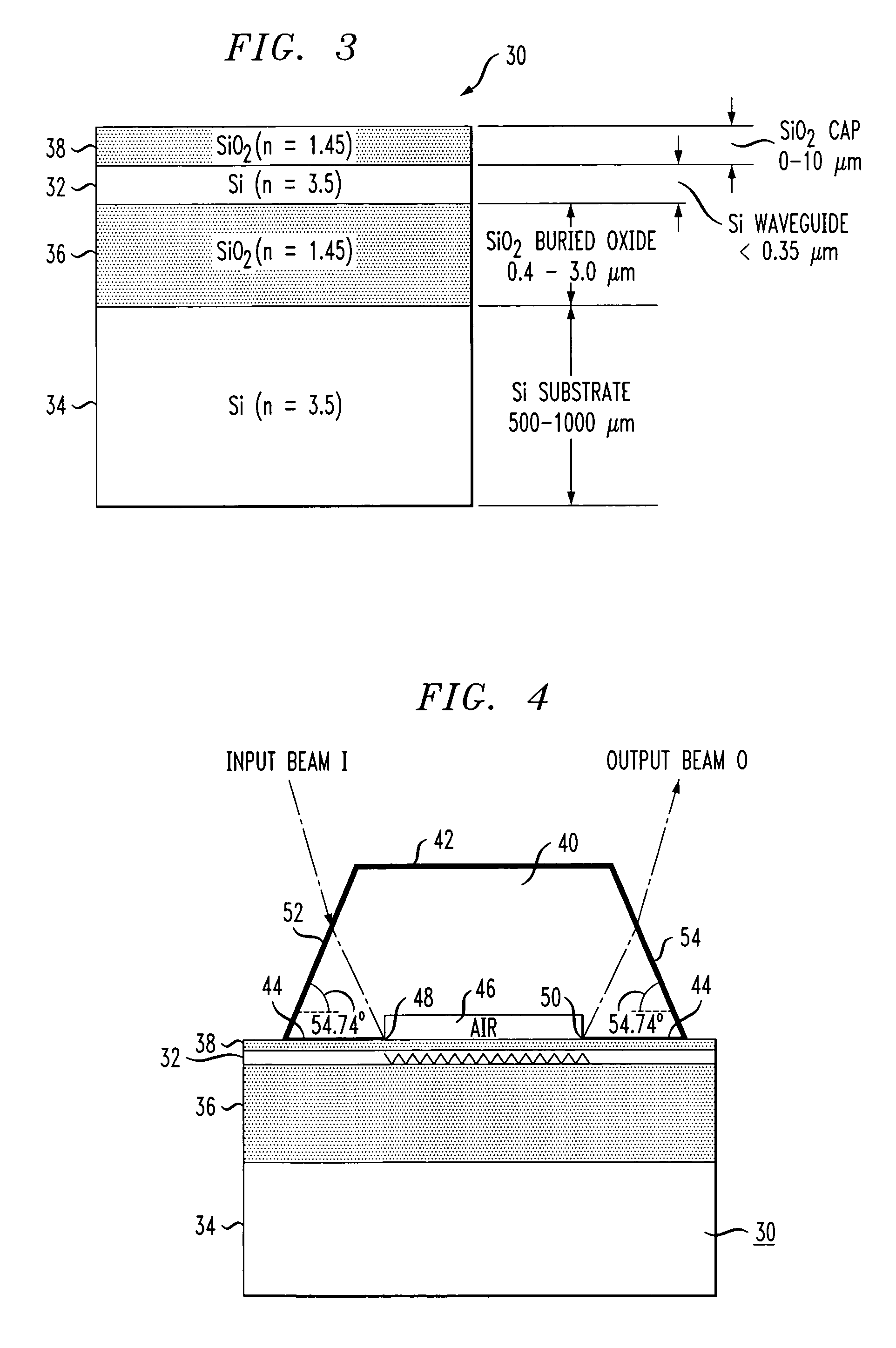
[0036]FIGS. 1 and 2 illustrate two well-known examples of prior art prism coupling arrangements that utilize the principle of evanescent coupling to introduce a light signal into a planar waveguide structure. In the arrangement of FIG. 1, a light beam is introduced from an external source to an input facet 10 of a prism 12 and thereafter propagates through prism 12, passes through an evanescent coupling medium 13 (in this case, air) and then into a waveguide 14. The light signal is then extracted from waveguide 14 by evanescently coupling light back out of waveguide 14 and into prism 12. Light is detected from output facet 16 of prism 12 via a photodetector 17 only when the angle of incidence fulfills the phase-matching condition determined by: (1) the polarization state of the input light signal; (2) the refractive indexes of prism 12, evanescent coupling medium 13, waveguide 14 and waveguide substrate 19; (3) the thickness (g) of evanescent coupling medium 13 and the thickness of ...


PUM


Abstract

A trapezoidal shaped single-crystal silicon prism is formed and permanently attached to an SOI wafer, or any structure including a silicon optical waveguide. In order to provide efficient optical coupling, the dopant species and concentration within the silicon waveguide is chosen such that the refractive index of the silicon waveguide is slightly less than that of the prism coupler (refractive index of silicon≈3.5). An intermediate evanescent coupling layer, disposed between the waveguide and the prism coupler, comprises a refractive index less than both the prism and the waveguide. In one embodiment, the evanescent coupling layer comprises a constant thickness. In an alternative embodiment, the evanescent coupling layer may be tapered to improve coupling efficiency between the prism and the waveguide. Methods of making the coupling arrangement are also disclosed.

Description

CROSS-REFERENCE TO RELATED APPLICATION[0001]This application claims the benefit of Provisional Application No. 60 / 459,349, filed Mar. 31, 2003.TECHNICAL FIELD[0002]The present invention relates to a light coupling arrangement for use with thin silicon optical waveguides and, more particularly to arrangements and methods of making silicon-based prism couplers that are permanently attached to silicon-based optoelectronic arrangements.BACKGROUND OF THE INVENTION[0003]To meet the bandwidth requirements of current and future high-speed applications, state-of-the-art telecommunication components and systems must provide a host of sophisticated signal processing and routing functions, both in the optical and electronic domains. As the complexity level increases, integration of more functions and components within a single package is required to meet system-level requirements and reduce the associated size and cost of the end system. It has been recognized for some time that the integrated ...

Claims


Application Information

Patent Timeline
IPC IPC(8): G02B6/34G02B6/42
CPCG02B6/4206
Inventor GHIRON, MARGARETGOTHOSKAR, PRAKASHMONTGOMERY, ROBERT KEITHPATEL, VIPULKUMARPATHAK, SOHAMSHASTRI, KALPENDUYANUSHEFSKI, KATHERINE A.
Owner CISCO TECH INC
Why Eureka
Try Eureka