Method for making an optical micromirror and micromirror or array of micromirrors obtained by said method

a technology of optical micromirrors and micromirrors, which is applied in the direction of piezoelectric/electrostrictive devices, chemical vapor deposition coatings, decorative arts, etc., can solve the problems of poor mechanical properties of amorphous or polycrystalline layers and unsatisfactory precision, and achieve the effect of greater freedom of realization

Inactive Publication Date: 2006-04-04
TEEM PHOTONICS
View PDF11 Cites 58 Cited by
  • Summary
  • Abstract
  • Description
  • Claims
  • Application Information

AI Technical Summary

Benefits of technology

[0041]The transfer technique used in this second embodiment makes possible the use of at least two wafers advantageously assembled using molecular adhesion techniques and also makes it possible to overcome the limitations of angular excursion without sacrificing precision relative to the thickness of the sacrificial layer(s) (whic

Problems solved by technology

The drawbacks of the prior art approaches are at several levels:First of all, unsatisfactory precision in angular excursion (typically between 10−1 and 10−2) as the result of the use of sacrificial layers produced by deposition techniques that do not have very high degrees of thickness control.For certain system architectures, in particular those used for optical routing purposes, all of thes

Method used


Image

  • Method for making an optical micromirror and micromirror or array of micromirrors obtained by said method
  • Method for making an optical micromirror and micromirror or array of micromirrors obtained by said method
  • Method for making an optical micromirror and micromirror or array of micromirrors obtained by said method

Examples


first embodiment

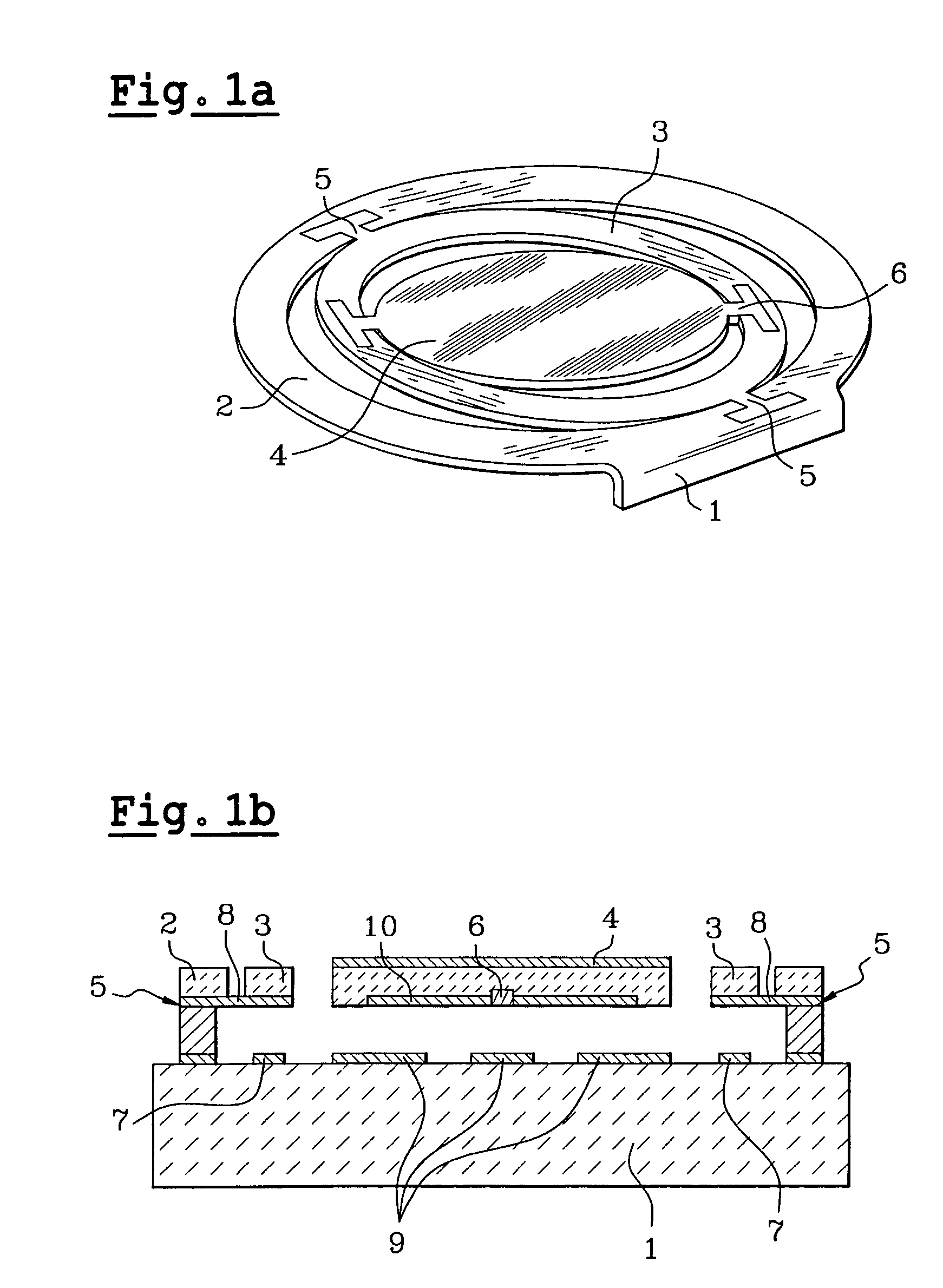
[0082]the micro-mirror of the invention that is implemented on a wafer is illustrated in the different FIG. 2.

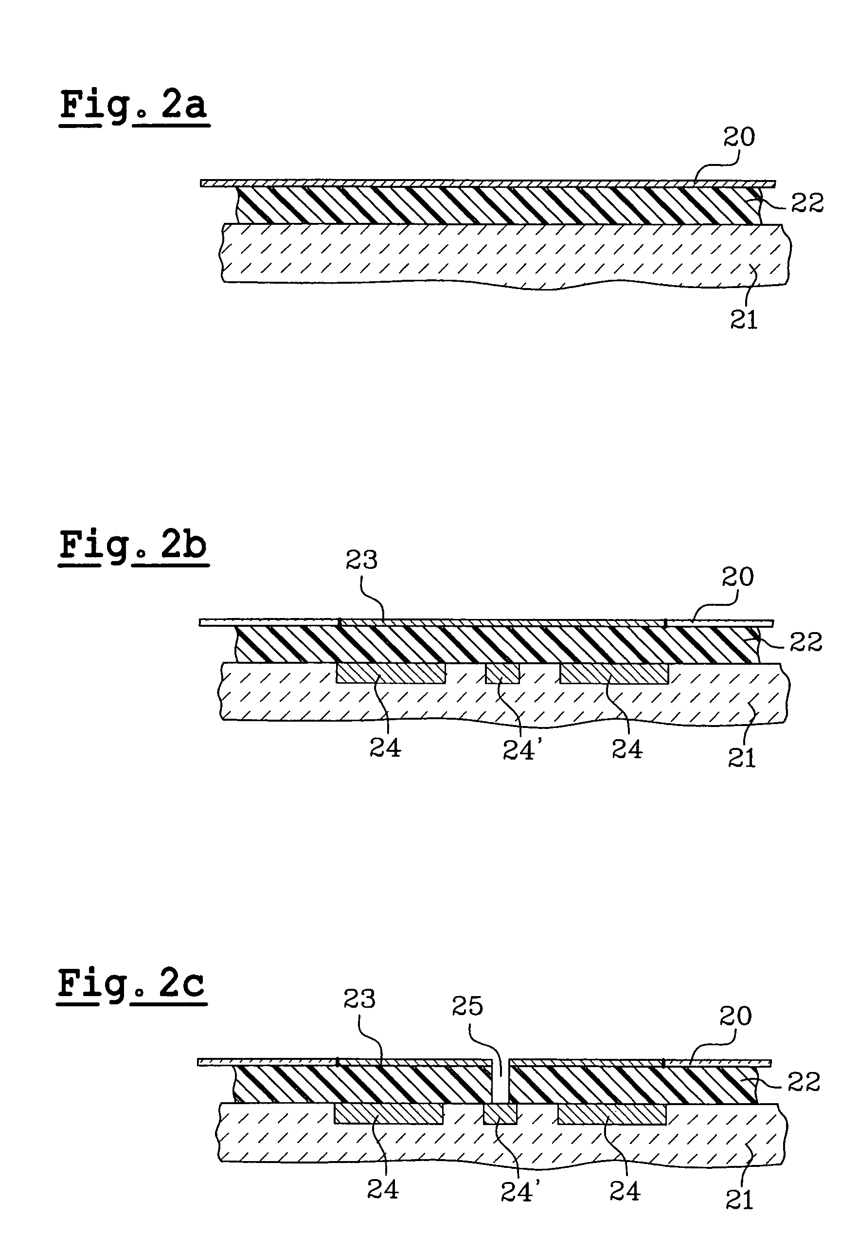
[0083]For this (see FIG. 2a in cross-section) a SOI (silicon on insulator) wafer is created or a wafer of this type available commercially is used.

[0084]In order to create this type of wafer, a non-doped silicon substrate 21 is used, onto which a dielectric layer 22 of thermal silica is grown. A surface monocrystalline silicon layer 20 is then deposited using any of the known deposition methods and in particular those for transferring a thin layer.

[0085]FIG. 2b represents the realization of the electrodes of the electrical control by the formation of different doped zones 24, 24′, and 23 in the superior part of the non-doped silicon substrate 21 and in the monocrystalline silicon surface layer 20. These zones are obtained by ionic implantation of dopant atoms (generally boron or phosphorus) at different energies according to the desired depth of localization, whether or not ...

second embodiment

[0100]the invention that carries out the steps of the method on two wafers A and B then which transfers these wafers is represented in FIGS. 3, 4, 5.

Preparation of the A Wafer

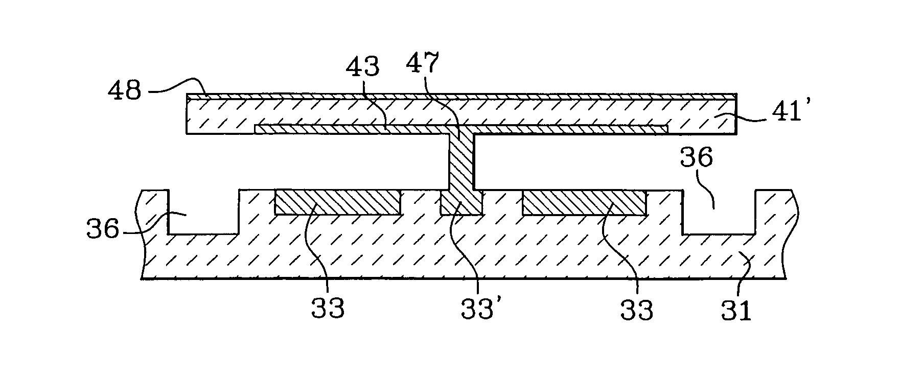
[0101]Using a mechanical support, for example an undoped silicon wafer 31 (FIG. 3a), the different electrodes 33, 33′ of the fixed part is realized by ion implantation of dopants whether or not followed by thermal annealing (FIG. 3b). FIG. 3c represents a thermal oxidation step of the substrate for forming a thermal oxide layer 32 of a perfectly controlled thickness and generally between 1 and 3 microns; in the course of this step done generally at high temperature, there is a diffusion of the dopants from the implanted zones and an increase of the volume occupied by these zones.

[0102]The steps represented in FIG. 3b and FIG. 3c can be reversed at the cost of augmentation of the implantation energies for realizing the doped zones 33 and 33′ (the ions implanted prior then cross the thermal silica layer).

[0103]FI...


PUM

PropertyMeasurementUnit
Fractionaaaaaaaaaa
Timeaaaaaaaaaa
Thicknessaaaaaaaaaa

Abstract

A method for manufacturing an optical micro-mirror including a fixed part and a moveable part, with a reflection device connected to the fixed part by an articulation mechanism. This method realizes a stack including a mechanical substrate, a first layer of thermal oxidation material, and at least one second layer of material for forming the moveable part, realizes the articulation mechanism, realizes the reflection device on the second layer, realizes the moveable part by etching of at least the second layer of material, and eliminates the thermal oxidation layer to liberate the moveable part. Such an optical micro-mirror may find possible applications to optical routing or image projection systems.

Description

FIELD OF THE INVENTION[0001]The invention relates to a method for manufacturing an optical micro-mirror and a micro-mirror or array of micro-mirrors obtained by the method of the invention. These micro-mirrors are capable of being electrically controlled.[0002]Micro-mirrors are used generally in systems implementing deflections of light beams and in particular in optical routing systems or in image projection systems.BACKGROUND OF THE INVENTION[0003]Electrically controlled micro-mirrors (most often using electrostatic, electromagnetic, piezoelectric, or thermoelastic forces) capable of generating digital or analog angular positions are known in the literature. They generally use hinge configurations making it possible, according to the complexity of the technological steps employed, to oscillate around an axis (simple hinge) or around two axes (double hinge) of rotation oriented most frequently orthogonally.[0004]FIG. 1a represents a view of such an electrostatically controlled micr...

Claims


Application Information

Patent Timeline
IPC IPC(8): B29D11/00H01L21/00B81B3/00B81C1/00G02B26/08
CPCB81B3/0062G02B26/0841B81B2201/045B81B2203/058B81B2203/0181
Inventor VALETTE, SERGE
Owner TEEM PHOTONICS
Why Eureka
Try Eureka