Plasma reactor with overhead RF electrode tuned to the plasma with arcing suppression

a plasma reactor and overhead rf electrode technology, applied in the field of rf plasma reactors, can solve the problems of reducing system reliability, reducing the output impedance of the rf generator, and reducing the reliability of the system,

Inactive Publication Date: 2006-04-18
APPLIED MATERIALS INC
View PDF114 Cites 54 Cited by
  • Summary
  • Abstract
  • Description
  • Claims
  • Application Information

AI Technical Summary

Benefits of technology

[0014]A plasma reactor for processing a semiconductor workpiece, includes a reactor chamber having a chamber wall and containing a workpiece support for holding the semiconductor workpiece, an overhead electrode overlying said workpiece support, the electrode comprising a portion of said chamber wall, an RF power generator for supplying power at a frequency of said generator to said overhead electrode and capable of maintaining a plasma within said chamber at a desired plasma ion density level. The overhead electrode has a capacitance such that said overhead electrode and the plasma formed in said chamber at said desired plasma ion density resonate together at an electrode-plasma resonant frequency, said frequency of said generator being at least near said electrode-plasma resonant frequency. The reactor further includes an insulating layer formed on a surface of said overhead electrode facing said workpiece support, a capacitive insulating layer between said RF power generator and said overhead electrode, and a metal foam layer overlying and contacting a surface of said overhead electrode that faces away from said workpiece support. The insulating layer provides a capacitance sufficient to suppress arcing within said gas injection ports, the capacitive insulating layer has a sufficient capacitance to block D.C. current from a plasma within said chamber from flowing through said overhead electrode, and the metal foam layer is of a sufficient thickness to suppress an axial electric field within said gas injection orifices.

Problems solved by technology

One problem in such reactors is that the output impedance of the RF generator, typically 50 Ohms, must be matched to the load impedance presented by the combination of the electrode and the plasma.
Otherwise the amount of RF power delivered to the plasma chamber will fluctuate with fluctuations in the plasma load impedance so that certain process parameters such as plasma density cannot be held within the required limits.
One problem with such impedance match circuits is that they must be sufficiently agile to follow rapid changes in the plasma load impedance, and therefore are relatively expensive and can reduce system reliability due to their complexity.
Another problem is that the range of load impedances over which the match circuit can provide an impedance match (the “match space”) is limited.
Of course, this ability is limited by the maximum forward power [of] which the generator is capable of producing.
If the difference in impedances increases (e.g., due to plasma impedance fluctuations during processing) so that the VSWR exceeds 3:1, then the RF generator can no longer control the delivered power, and control over the plasma is lost.
As a result, the process is likely to fail.
A related problem is that the load impedance itself is highly sensitive to process parameters such as chamber pressure, plasma source power level, source power frequency and plasma density.
This limits the range of such process parameters (the “process window”) within which the plasma reactor must be operated to avoid an unacceptable impedance mismatch or avoid fluctuations that take load impedance outside of the match space.
Likewise, it is difficult to provide a reactor which can be operated outside of a relatively narrow process window and process use, or one that can handle many process applications.
Another related problem is that the load impedance is also affected by the configuration of the reactor itself, such as dimensions of certain mechanical features and the conductivity or dielectric constant of certain materials within the reactor.
This makes it difficult to maintain uniformity among different reactors of the same design due to manufacturing tolerances and variations in materials.
As a result, with a high system Q and correspondingly small impedance match space, it is difficult to produce any two reactors of the same design which exhibit the same process window or provide the same performance.
Another problem is inefficient use of the RF power source.
Plasma reactors are known to be inefficient, in that the amount of power delivered to the plasma tends to be significantly less than the power produced by the RF generator.
As a result, an additional cost in generator capability and a trade-off against reliability must be incurred to produce power in excess of what is actually required to be delivered into the plasma.
This poses a risk of the plasma discharge removing material of the overhead electrode or showerhead from the interior surfaces of the gas injection ports.
The species, e.g. metallic species, thus introduced into the plasma can contaminate the surface of the wafer or workpiece and damage the microelectronic devices being fabricated thereon.
The overhead electrode may suffer wear from being in contact with plasma, particularly since it is both an anode for the bias power and a cathode for the source power and is therefore subject to RF and DC currents.
A problem often found in plasma reactors is the generation of second and third harmonics within the plasma sheath.
The presence of such harmonics changes plasma behavior in such a way that process performance is impaired in the presence of such harmonics.
Specifically, process control to avoid etch stop or over-etching becomes more difficult, and the etch rate is reduced.

Method used


Image

  • Plasma reactor with overhead RF electrode tuned to the plasma with arcing suppression
  • Plasma reactor with overhead RF electrode tuned to the plasma with arcing suppression
  • Plasma reactor with overhead RF electrode tuned to the plasma with arcing suppression

Examples


Embodiment Construction

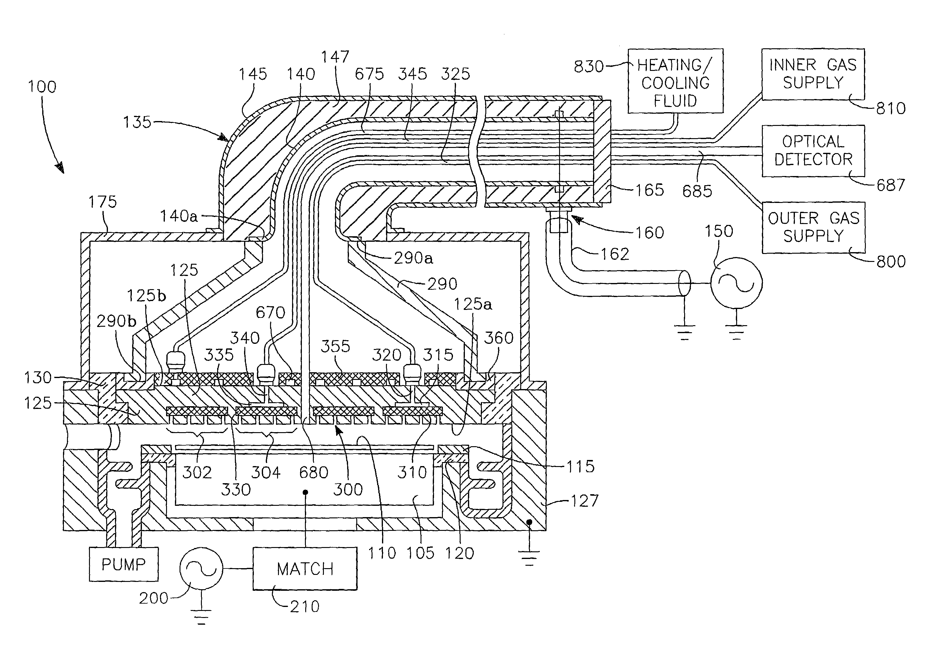
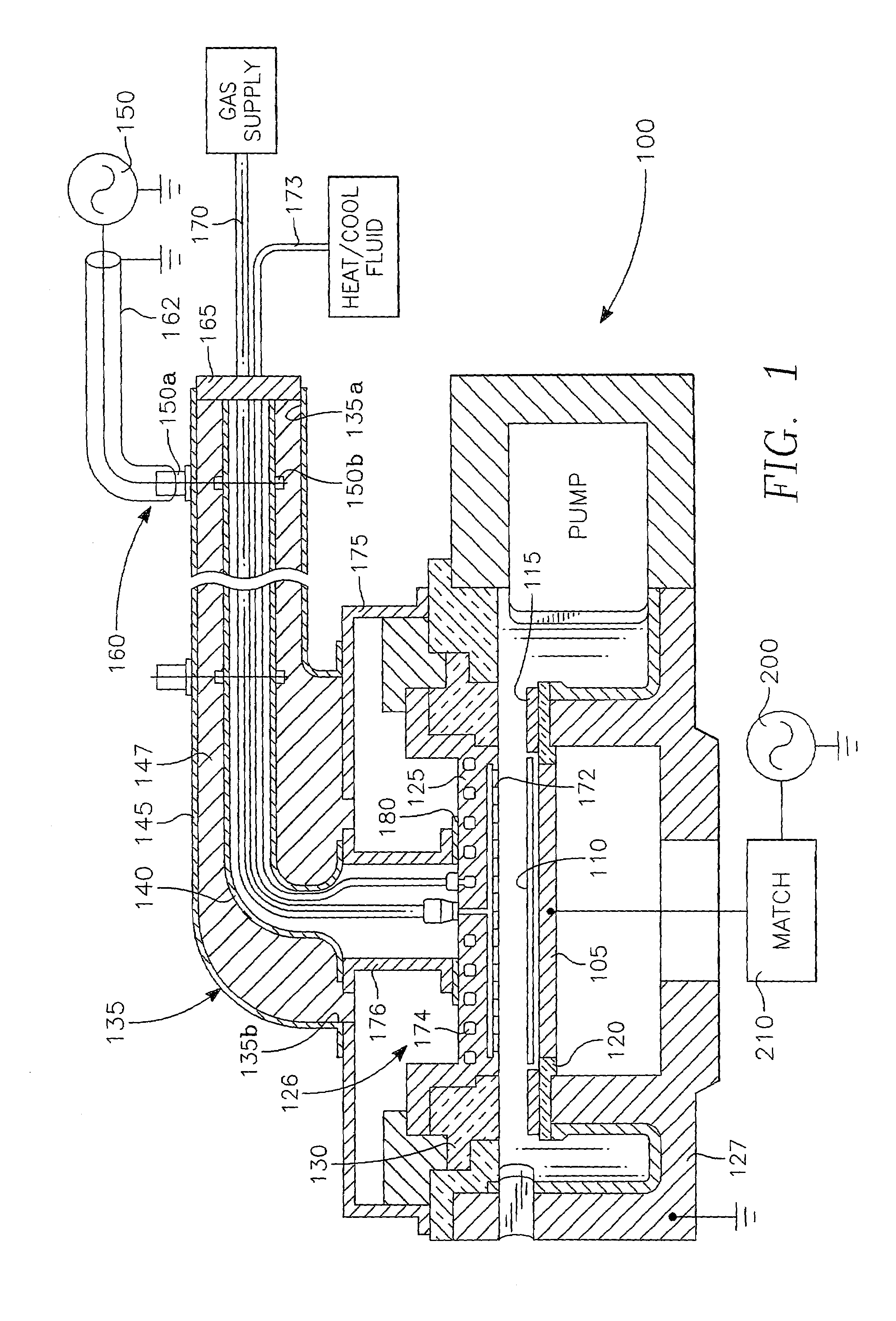
[0029]Referring to FIG. 1, a plasma reactor includes a reactor chamber 100 with a wafer support 105 at the bottom of the chamber supporting a semiconductor wafer 110. A semiconductor ring 115 surrounds the wafer 110. The semiconductor ring 115 is supported on the grounded chamber body 127 by a dielectric (quartz) ring 120. In one embodiment, this is of a thickness of 10 mm and dielectric constant of 4. The chamber 100 is bounded at the top by a disc shaped overhead aluminum electrode supported at a predetermined gap length above the wafer 110 on grounded chamber body 127 by a dielectric (quartz) seal. The overhead electrode 125 also may be a metal (e.g., aluminum) which may be covered with a semi-metal material (e.g., Si or SiC) on its interior surface, or it may be itself a semi-metal material. An RF generator 150 applies RF power to the electrode 125. RF power from the generator 150 is coupled through a coaxial cable 162 matched to the generator 150 and into a coaxial stub 135 con...


PUM

PropertyMeasurementUnit
impedanceaaaaaaaaaa
currentaaaaaaaaaa
thicknessaaaaaaaaaa

Abstract

A plasma reactor for processing a semiconductor workpiece, includes a reactor chamber having a chamber wall and containing a workpiece support for holding the semiconductor workpiece, an overhead electrode overlying said workpiece support, the electrode comprising a portion of said chamber wall, an RF power generator for supplying power at a frequency of said generator to said overhead electrode and capable of maintaining a plasma within said chamber at a desired plasma ion density level. The overhead electrode has a capacitance such that said overhead electrode and the plasma formed in said chamber at said desired plasma ion density resonate together at an electrode-plasma resonant frequency, said frequency of said generator being at least near said electrode-plasma resonant frequency. The reactor further includes an insulating layer formed on a surface of said overhead electrode facing said workpiece support, a capacitive insulating layer between said RF power generator and said overhead electrode, and a metal foam layer overlying and contacting a surface of said overhead electrode that faces away from said workpiece support.

Description

CROSS-REFERENCE TO RELATED APPLICATIONS:[0001]This application is a continuation in part of U.S. application Ser. No. 09 / 527,342 filed Mar. 17, 2000 now U.S. Pat. No. 6,528,751 by Daniel Hoffman et al., entitled Plasma Reactor with Overhead RF Electrode Tuned to the Plasma and assigned to the present assignee.BACKGROUND OF THE INVENTION[0002]An RF plasma reactor is used to process semiconductor wafers to produce microelectronic circuits. The reactor forms a plasma within a chamber containing the wafer to be processed. The plasma is formed and maintained by application of RF plasma source power coupled either inductively or capacitively into the chamber. For capacitive coupling of RF source power into the chamber, an overhead electrode (facing the wafer) is powered by an RF source power generator.[0003]One problem in such reactors is that the output impedance of the RF generator, typically 50 Ohms, must be matched to the load impedance presented by the combination of the electrode an...

Claims


Application Information

Patent Timeline
Patent Type & Authority Patents(United States)
IPC IPC(8): B23K10/00H01J37/32H05H1/46H01L21/205H01L21/3065
CPCH01J37/32183H01J37/32082H01J37/32
Inventor HOFFMAN, DANIEL J.YIN, GERALD ZHEYAOYE, YANKATZ, DANBUCHBERGER, JR., DOUGLAS A.ZHAO, XIAOYECHIANG, KANG-LIEHAGEN, ROBERT B.MILLER, MATTHEW L.
Owner APPLIED MATERIALS INC
Why Eureka
Try Eureka