Low-pass filter for a PLL, phase-locked loop and semiconductor integrated circuit

a semiconductor integrated circuit and low-pass filter technology, applied in the field of low-pass filter, can solve the problems of substantially impossible externally providing a large capacitive element on an ic card, reduce the circuit area of the pll, and change the characteristic of the filter, so as to achieve the effect of keeping the dumping factor constan

Inactive Publication Date: 2006-04-18
PANASONIC CORP
View PDF10 Cites 99 Cited by
  • Summary
  • Abstract
  • Description
  • Claims
  • Application Information

AI Technical Summary

Benefits of technology

[0016]In the low-pass filter having the aforementioned architecture, the given rate of the second current to the first current is changed so as to accordingly change the transfer characteristic of the second filtering means, and hence, the second filtering means outputs the second voltage equivalent to the original voltage. Therefore, the low-pass filter apparently keeps its original transfer characteristic. In other words, even when the structure of the second filtering means is changed so as to reduce the circuit scale and hence the transfer characteristic is changed, the filtering characteristic of the low-pass filter can be prevented from changing by changing the given rate in accordance with the changed transfer characteristic. Accordingly, the invention can realize a low-pass filter that has a filtering characteristic equivalent to that of a conventional one and has a circuit area smaller than the conventional one.
[0017]In the low-pass filter of this invention, the given rate is preferably a positive number smaller than 1. Thus, the second current to be generated is smaller than the first current, and hence, a capacitive element with a small capacitance value can be employed as the capacitive element used in the second filtering means. Accordingly, the second filtering means can be downsized, resulting in reducing the circuit area of the low-pass filter.
[0021]In the low-pass filter of this invention, preferably, the first and second semiconductor elements are respectively first and second transistors for providing the first and second conductance in accordance with supplied first and second bias currents, respectively. The first and second bias currents are changed in amplitudes thereof on the basis of a common bias control signal. The change of the first and second bias currents means change of the first and second conductance. Since the first and second conductance are thus changed, the filtering characteristic of the low-pass filter can be dynamically varied. In addition, the filtering characteristic can be varied on the basis of the bias control signal commonly used for the first and second bias currents. Accordingly, there is no need to provide a resistor ladder circuit for varying the filtering characteristic of the low-pass filter, and hence, the circuit scale can be further reduced. Furthermore, particularly when the low-pass filter is used as a loop filter for a phase-locked loop or the like, the dumping factor can be effectively and easily adjusted in accordance with the bias control signal.
[0025]On the other hand, the feedback system of this invention includes a charge pump circuit for generating a charge current on the basis of a phase difference between an input clock and a clock resulting from feedback; a loop filter for accepting the charge current as an input; and output clock generating means for generating an output clock on the basis of an output signal from the loop filter. The loop filter includes first filtering means for accepting the charge current as an input and outputting a first voltage; a circuit element included in the first filtering means for allowing a first current to flow in accordance with the first voltage; current generating means for generating a second current at a given rate to the first current; second filtering means for accepting the second current as an input and outputting a second voltage; and adding means for adding the first voltage and the second voltage and outputting the output signal. Thus, the low-pass filter having the architecture shown in FIG. 1 is used as the loop filter of the feedback system, and hence, the circuit area of the feedback system can be reduced.
[0029]Preferably, the circuit element is capable of changing conductance thereof, and the feedback system further includes bias controlling means for changing the conductance of the circuit element and the charge current in accordance with a common bias control signal. Thus, the conductance of the circuit element and the charge current are both changed on the basis of the common bias control signal, and therefore, the dumping factor can be kept constant.

Problems solved by technology

The passive filter shown in FIG. 33(a) has a disadvantage that its characteristic is changed when another circuit is connected at a subsequent stage.
In some application products of PLLs that are difficult to externally provide a large capacitive element, it is significant to reduce the circuit area of the PLL.
Accordingly, it is substantially impossible to externally provide a large capacitive element on an IC card, and hence, the circuit area reduction of the PLL is a problem to be indispensably solved.
Furthermore, since a large number of PLLs are used in a microprocessor, the circuit area of the PLLs largely affects the circuit area of the whole microprocessor.

Method used


Image

  • Low-pass filter for a PLL, phase-locked loop and semiconductor integrated circuit
  • Low-pass filter for a PLL, phase-locked loop and semiconductor integrated circuit
  • Low-pass filter for a PLL, phase-locked loop and semiconductor integrated circuit

Examples


embodiment 1

(Embodiment 1)

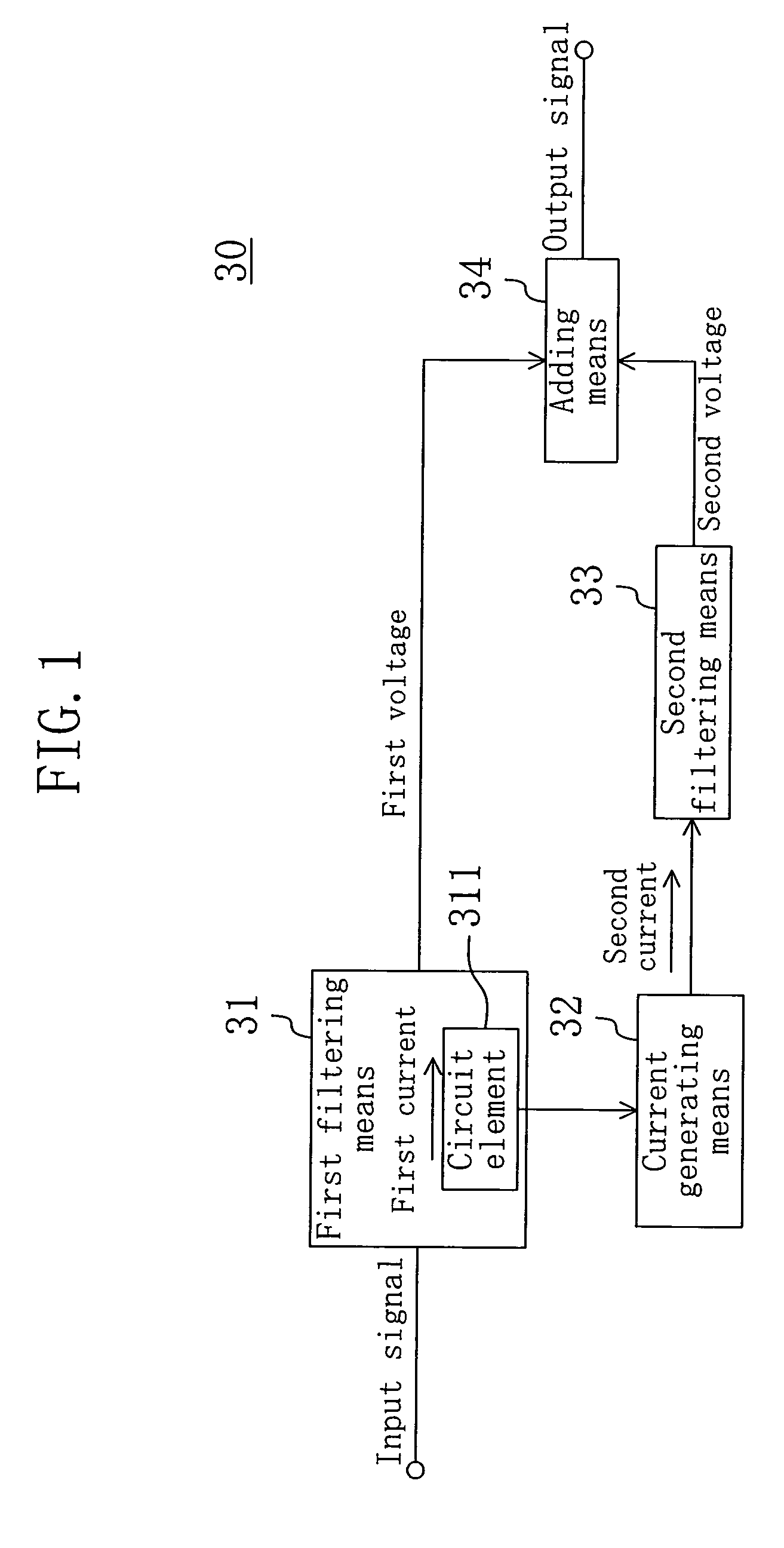
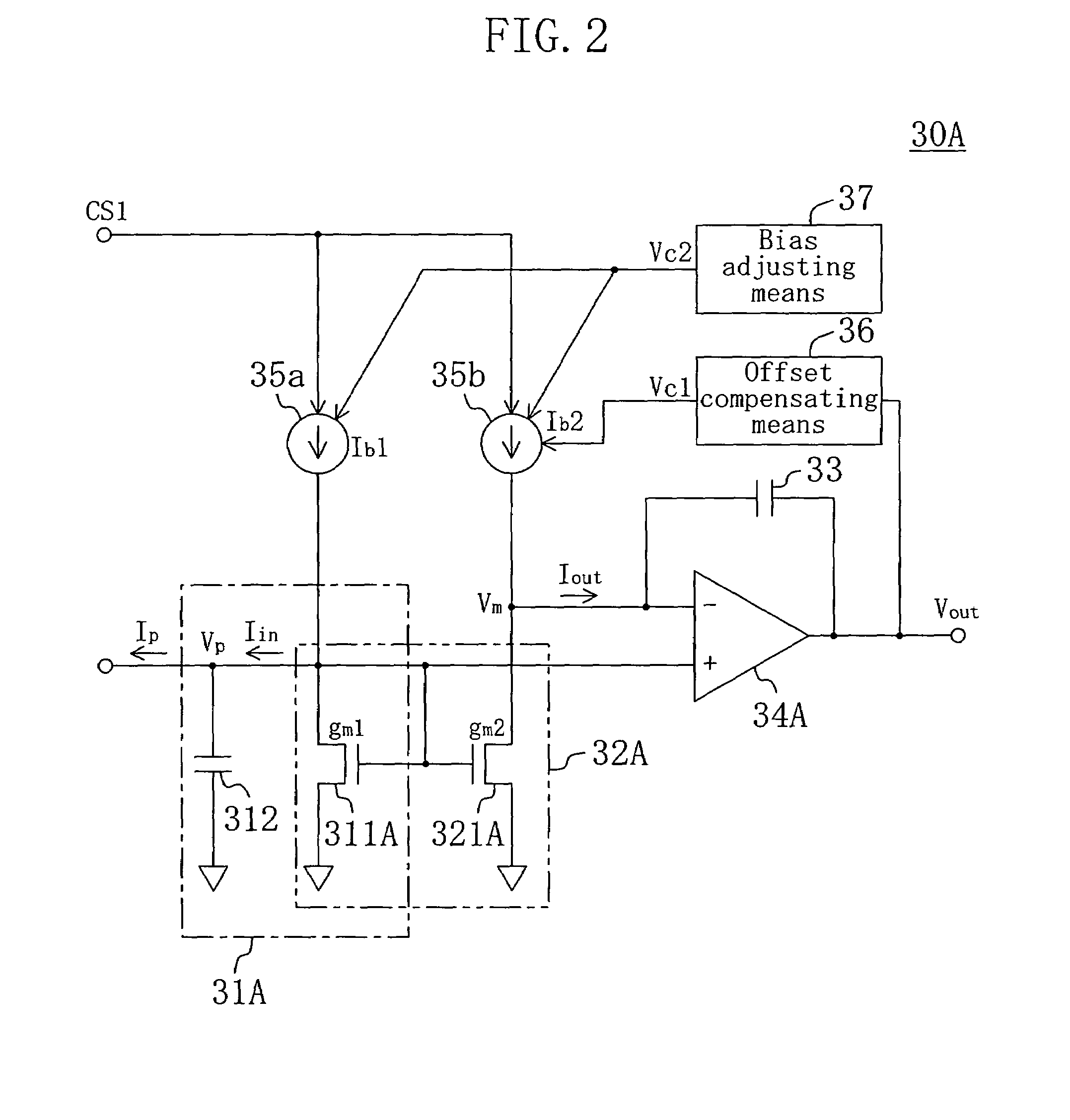
[0070]FIG. 2 shows a low-pass filter according to Embodiment 1 of the invention. The low-pass filter 30A of this embodiment is a second-order active filter including a capacitive element 312, a current mirror circuit 32A, a capacitive element 33, an operational amplifier 34A, current sources 35a and 35b, offset compensating means 36 and bias adjusting means 37. The low-pass filter 30A can be constructed as a semiconductor integrated circuit.

[0071]The low-pass filter 30A is applicable to, for example, the PLL shown in FIG. 32. In this application, the low-pass filter 30A accepts, as an input, a charge current Ip (whereas in a reverse direction to that shown in FIG. 32) from the charge pump circuit 20 and outputs a control voltage Vout, so as to control the voltage controlled oscillator 40.

[0072]The current mirror circuit 32A corresponds to the current generating means of this invention. The current mirror circuit 32A has, on its input side, a field effect transistor 311...

embodiment 2

(Embodiment 2)

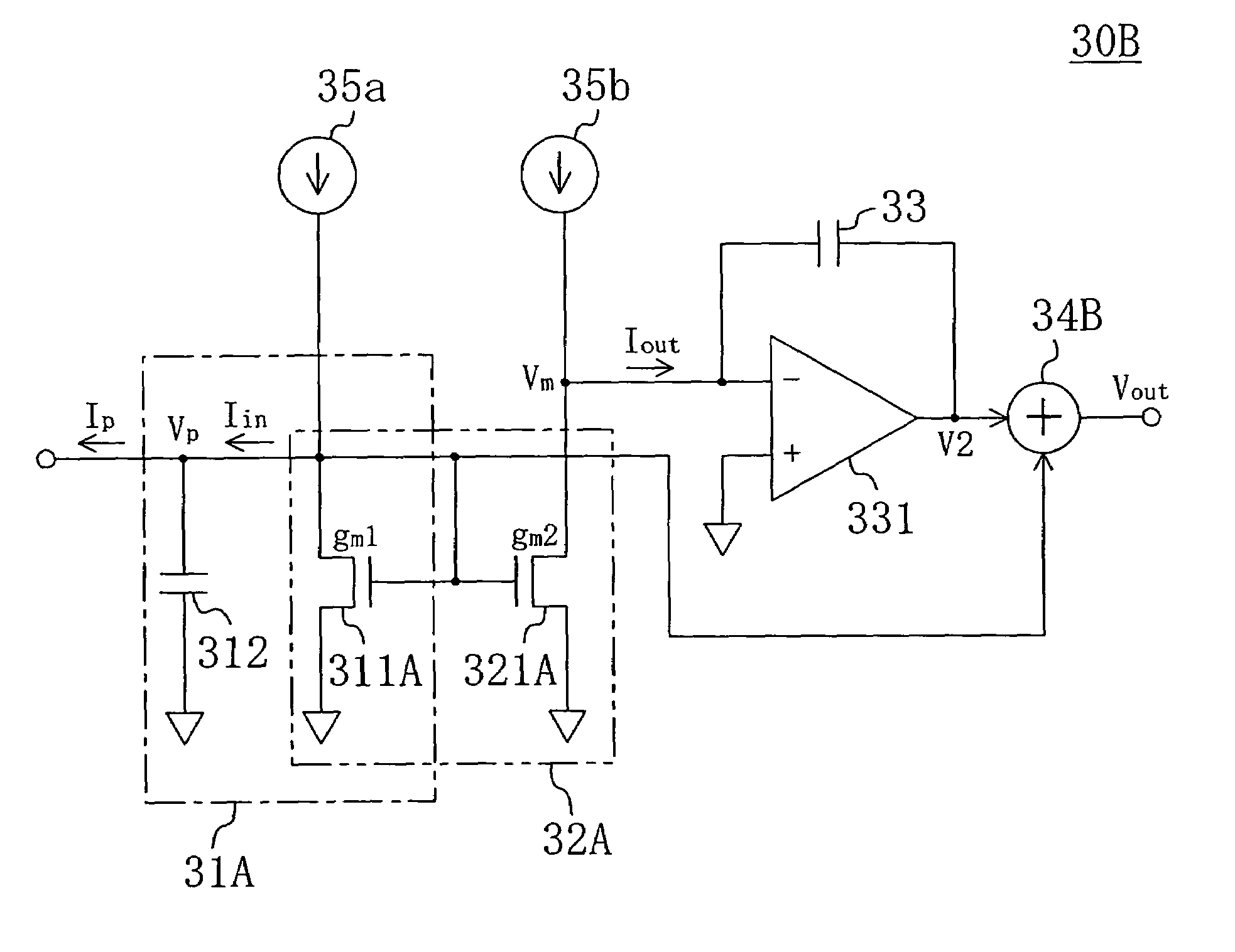
[0113]FIG. 11 shows a low-pass filter according to Embodiment 2 of the invention. The low-pass filter 30B of this embodiment is obtained by modifying the adding means of the low-pass filter 30A of Embodiment 1. Herein, a difference from Embodiment 1 alone will be described. The description of elements similar to those of Embodiment 1 is omitted by referring to them with like reference numerals used in FIG. 2.

[0114]In the low-pass filter 30B, an operational amplifier 331 has the capacitive element 33 in its negative feedback portion, and accepts, as an input, a reference voltage at its non-inverting input terminal and outputs a second voltage V2. In other words, the capacitive element 33 and the operational amplifier 331 together correspond to the second filtering means in this embodiment.

[0115]An adder 34B corresponds to the adding means in this embodiment. The adder 34B accepts the first voltage Vp and the second voltage V2 as inputs, and adds these voltages to output...

embodiment 3

(Embodiment 3)

[0117]FIG. 12 shows a low-pass filter according to Embodiment 3 of the invention. The low-pass filter 30C of this embodiment is obtained by modifying the adding means of the low-pass filter 30A of Embodiment 1. Herein, a difference from Embodiment 1 alone will be described. The description of elements similar to those of Embodiment 1 is omitted by referring to them with like reference numerals used in FIG. 2.

[0118]In the low-pass filter 30C, one end of the capacitive element 33 is set to a reference voltage. Thus, the capacitive element 33 accepts the second current Iout as an input and outputs a second voltage V2 with the inverted polarity.

[0119]The adding means of this embodiment is an operational transconductance amplifier (OTA) 34C. The OTA 34C accepts, as inputs, the first voltage Vp at its non-inverting input terminal and the second voltage V2 with the inverted polarity at its inverting input terminal, and outputs a third current Iout2 as the output signal of the...


PUM


Abstract

The invention provides a low-pass filter suitably used as a loop filter for a PLL or a DLL that has a filtering characteristic equivalent to that of a conventional one and can be realized in a smaller circuit area. The low-pass filter includes first filtering means (31) for accepting, as an input, an input signal to the low-pass filter and outputting a first voltage; a circuit element (311) included in the first filtering means (31) for allowing a first current to flow in accordance with the first voltage; current generating means (32) for generating a second current at a given rate to the first current; second filtering means (33) for accepting, as an input, the second current and outputting a second voltage; and adding means (34) for adding the first voltage and the second voltage and outputting an output signal of the low-pass filter, in which the second current is set to be smaller than the first current.

Description

TECHNICAL FIELD[0001]The present invention relates to a low-pass filter, and more particularly, it relates to a low-pass filter suitably used as a loop filter in a phase-locked loop and the like, and a technique for a phase-locked loop including such a low-pass filter.BACKGROUND ART[0002]A phase-locked loop (hereinafter referred to as a “PLL”) is now an indispensable element in a semiconductor integrated circuit system and is included in almost all LSIs. Also, there are broad ranges of applications of PLLs extending over various fields such as communications equipment, microprocessors and IC cards.[0003]FIG. 32 shows the architecture of a general charge pump type PLL. The outline of the PLL will now be described with reference to this drawing. A phase comparator 10 compares an input clock CKin supplied to the PLL with a feedback clock CKdiv so as to output an up signal UP and a down signal DN in accordance with a phase difference between these clocks. A charge pump circuit 20 output...

Claims


Application Information

Patent Timeline
Patent Type & Authority Patents(United States)
IPC IPC(8): H03K5/00H03H11/04H03H11/12H03L7/08H03L7/081H03L7/089H03L7/093H03L7/107
CPCH03L7/0812H03L7/0891H03L7/093H03L7/0896H03L7/0893H03L7/0816
Inventor DOSHO, SHIROYANAGISAWA, NAOSHITOYAMA, MASAOMIUMEHARA, KEIJIROFUKUI, MASAHIROYOSHIKAWA, TAKEFUMIIWATA, TORUSAKIYAMA, SHIROSUZUKI, RYOICHI
Owner PANASONIC CORP
Why Eureka
Try Eureka