Eureka AIR delivers breakthrough ideas for toughest innovation challenges, trusted by R&D personnel around the world.

Methods of forming capacitor constructions

Active Publication Date: 2006-04-25
MICRON TECH INC
View PDF46 Cites 27 Cited by
  • Summary
  • Abstract
  • Description
  • Claims
  • Application Information

AI Technical Summary

Benefits of technology

[0008]In one aspect, the invention encompasses a capacitor construction which includes a first capacitor electrode having a layer comprising titanium and nitrogen. A layer comprising aluminum oxide is over the l

Problems solved by technology

Although the high-k dielectric materials described above can provide numerous advantages when utilized in capacitor constructions, there are difficulties associated with the materials which can offset the benefits gained by utilizing the materials.
One problem encountered when incorporating high-k materials into current DRAM cell designs is that chemical reactivity between the high-k materials and other materials of a DRAM cell can impede performance of the cell, and even destroy operability of the cell.
The oxidized electrode components can have reduced electrical conductivity relative to non-oxidized components, which can impair operability of the resulting capacitor cell, and in some cases can lower the total capacitance of resulting capacitor below acceptable tolerances.

Method used


Image

  • Methods of forming capacitor constructions
  • Methods of forming capacitor constructions
  • Methods of forming capacitor constructions

Examples


Embodiment Construction

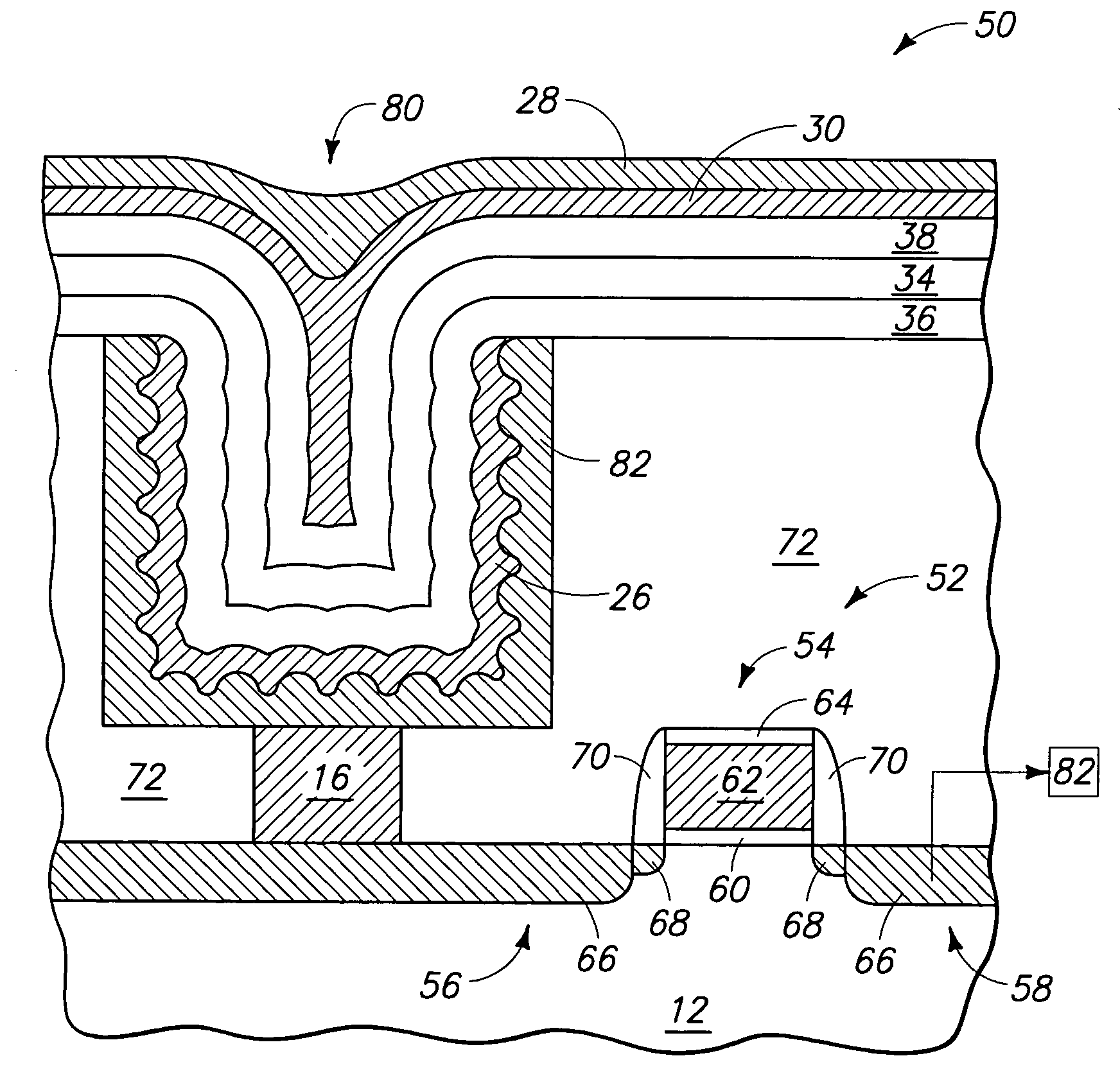
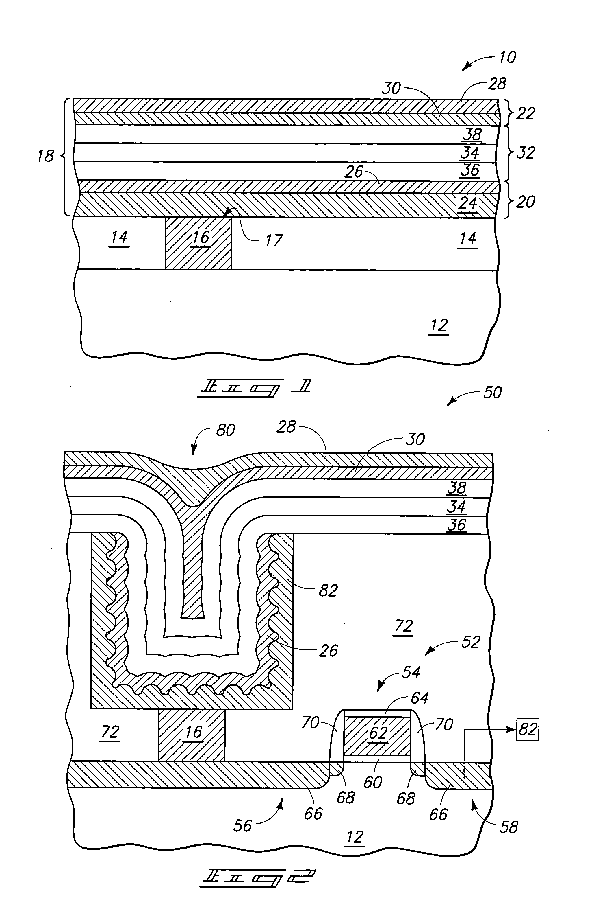
[0019]This disclosure of the invention is submitted in furtherance of the constitutional purposes of the U.S. Patent Laws “to promote the progress of science and useful arts” (Article 1, Section 8).

[0020]The invention includes a recognition that it can be useful to utilize aluminum oxide (Al2O3) dielectric material as a barrier layer between a capacitor electrode and a high-k dielectric material other than aluminum oxide in applications in which the capacitor electrode comprises titanium and nitrogen. In particular applications, the capacitor electrode can comprise one or both of titanium nitride (TiN) and boron-doped titanium nitride (TiBN). The high-k dielectric material can comprise, for example, one or more of Ta2O5, HfOx, ZrOy, barium strontium titanate, strontium titanate, and lead zirconate titanate, where x and y are numbers greater than 0. The capacitor constructions can be metal insulator metal (MIM) constructions, and in particular aspects both electrodes of the capacitor...


PUM

PropertyMeasurementUnit
Electrical conductoraaaaaaaaaa

Abstract

The invention includes capacitor constructions comprising a layer of aluminum oxide between a high-k dielectric material and a layer comprising titanium and nitrogen. The layer comprising titanium and nitrogen can be, for example, titanium nitride and / or boron-doped titanium nitride. The capacitor constructions can be incorporated into DRAM cells, which in turn can be incorporated into electronic systems. The invention also includes methods of forming capacitor constructions.

Description

RELATED PATENT DATA[0001]This patent resulted from a divisional application of U.S. patent application Ser. No. 10 / 442,509, which was filed May 20, 2003.TECHNICAL FIELD[0002]The invention pertains to capacitor constructions and methods of forming capacitor constructions.BACKGROUND OF THE INVENTION[0003]Capacitor constructions are common circuit devices. Capacitor constructions are utilized in, for example, dynamic random access memory (DRAM) cells of integrated circuits. The DRAM cells typically comprise a charge storage capacitor coupled to an access device, with the typical access device being a metal-oxide-semiconductor field effect transistor (MOSFET).[0004]A continuing goal in integrated circuit device fabrication is to increase performance of circuit devices without increasing the amount of real estate consumed by the devices. For capacitor devices, such goal can manifest as a desire to increase the total charge capacity of a capacitor device without significantly affecting th...

Claims


Application Information

Patent Timeline
IPC IPC(8): H01L21/8242H01L21/00H01G4/12H01G4/228H01G4/33H01L21/02H01L21/316H01L21/8234H01L23/522H01L27/115
CPCH01G4/1209H01G4/228H01G4/33H01L28/56H01L28/75H01L2924/0002H01L21/31637H01L21/31641H01L21/31645H01L21/31691H01L23/5223H01L27/10852H01L27/11502H01L2924/00H01L28/40H10B12/033H10B53/00H01L21/02183H01L21/02189H01L21/02181H01L21/02197H01L21/02178H01L21/0228
Inventor BASCERI, CEMGRAETTINGER, THOMAS M.
Owner MICRON TECH INC
Why Eureka
Eureka Blog
Learn More