Charge detecting device

a detection device and charge technology, applied in the field of charge detection devices, can solve the problems of small pixel opening ratio, difficulty in reducing a chip size, and reducing conversion efficiency (q/cfd), and achieve the effect of large dynamic range of output voltage, low cost and high efficiency

Inactive Publication Date: 2006-04-25
COLLABO INNOVATIONS INC
View PDF6 Cites 5 Cited by
  • Summary
  • Abstract
  • Description
  • Claims
  • Application Information

AI Technical Summary

Benefits of technology

[0013]Therefore, with the foregoing in mind, it is an object of the present invention to provide a charge detecting device that can convert an accumulated charge to a voltage at a low voltage and a high efficiency, and has a large dynamic range of an output voltage and satisfactory linearity of a conversion efficiency.
[0016]According to the above configuration, even when a supply voltage is lowered, a charge can be converted to a voltage with a high conversion efficiency, i.e., a high conversion efficiency can be maintained in a large dynamic range.
[0017]It is preferable that the second region is depleted in a period from a time immediately after the reset voltage is applied at least to a time when a saturated charge is accumulated. According to this, the linearity characteristics can be made satisfactory by suppressing the fluctuation in a diffusion floating capacitance in the charge accumulating portion, and a large dynamic range can be maintained.
[0022]According to the present invention, a charge detecting device can be provided, which can convert a charge accumulated in a photodiode in a solid-state imaging apparatus at a low voltage and a high efficiency, and has a large dynamic range of an output voltage and satisfactory linearity of a conversion efficiency, due to the small dependency of the conversion efficiency on an accumulated charge amount.

Problems solved by technology

However, on the other hand, the APS has problems of a small pixel opening ratio and difficulty in reducing a chip size that determines the size of an optical system, due to the large number of elements per pixel.
Therefore, there is a problem that a conversion efficiency (Q / Cfd) is decreased, and an output voltage is lowered.
This contradicts the decrease in voltage that is required in a miniaturized MOS transistor, which makes it impossible to satisfy transistor characteristics.
More specifically, the linearity of a conversion efficiency is degraded.

Method used


Image

  • Charge detecting device
  • Charge detecting device
  • Charge detecting device

Examples


example 1

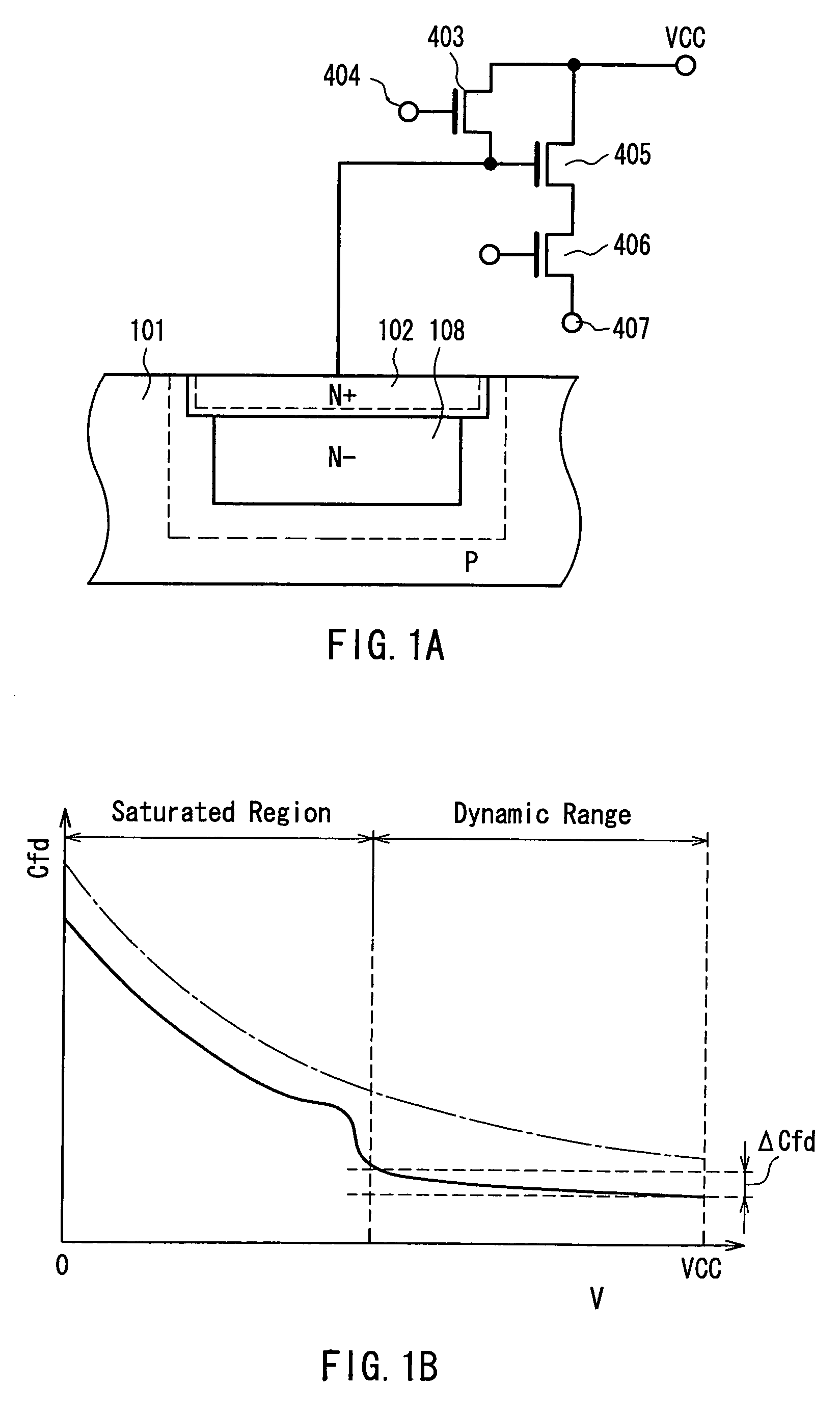
[0031]FIG. 1A is a view showing a cross-sectional configuration of a semiconductor of a photoelectric converter and a configuration of an output circuit in a charge detecting device according to Example 1 of the present invention. In FIG. 1A, portions having the same configurations and functions as those in FIG. 4A referred to in the description of the conventional example are denoted with the same reference numerals as those therein, and their description will be omitted here. In FIG. 1A, broken lines represent the ends of a depletion layer.

[0032]The photoelectric converter is configured in such a manner that an N-layer 108 of a photodiode is formed on a P-type semiconductor substrate (or a P-type well) 101, and an N-layer 102 of the photodiode is formed on the N-layer 108 so that the surface has a high impurity concentration. The photoelectric converter also functions as a diffusion floating region that also works as a charge accumulating portion. The photoelectric converter is co...

example 2

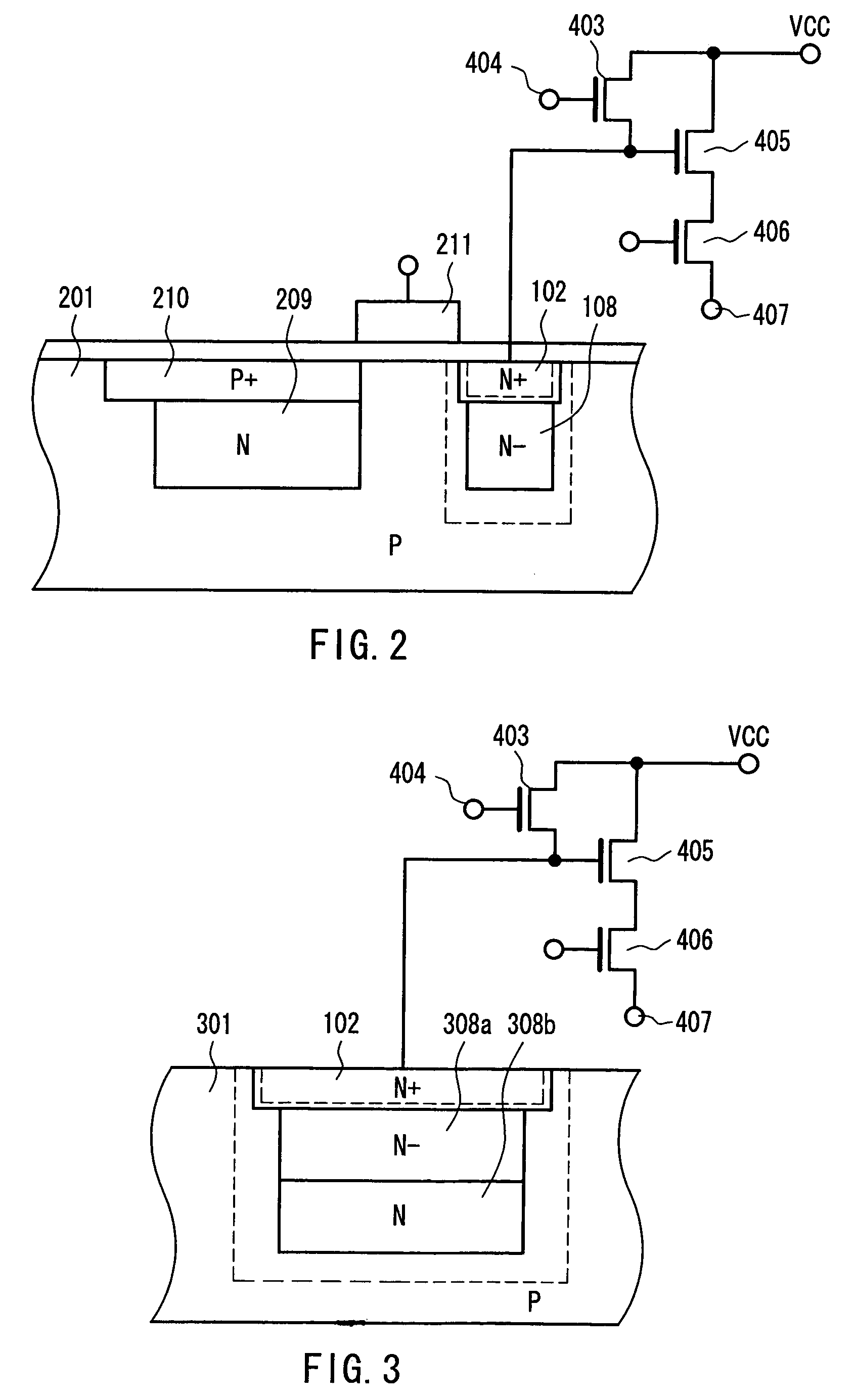
[0044]FIG. 2 shows a cross-sectional configuration of a semiconductor and a configuration of an output circuit in the case where the charge detecting device of Example 1 is applied to a CCD sensor as a solid-state imaging apparatus according to Example 2 of the present invention. In FIG. 2, the portions having the same configurations and functions as those in FIG. 1A referred to in the description of Example 1 are denoted with the same reference numerals as those therein, and their description will be omitted. In FIG. 2, broken lines represent the ends of a depletion layer.

[0045]In FIG. 2, a buried-type photodiode is used, in which the surface of an N-layer 209 of a photodiode that is used generally in a CCD sensor is formed of a high concentration P-layer (P+ layer) 210. A charge / voltage converting portion with high sensitivity at a low voltage according to Example 1 is connected to an output circuit via a read gate 211 interposed therebetween. In this example, a signal charge is a...

example 3

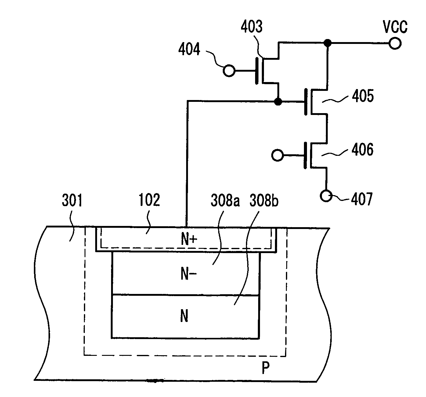
[0046]FIG. 3 shows a cross-sectional configuration of a semiconductor and a configuration of an output circuit of a photoelectric converter in a charge detecting device according to Example 3 of the present invention. In FIG. 3, portions having the same configurations and functions as those in FIG. 1A referred to in the description of Example 1 are denoted with the same reference numerals as those therein, and their description will be omitted here. In FIG. 3, broken lines represent the ends of a depletion layer.

[0047]The present example is obtained by further improving the configuration of Example 1, and is the most important and preferable example of a low concentration N-layer region in the present invention. The low concentration N-layer region is composed of two regions. A low concentration N-layer region (N−) 308a on a surface side is formed so as to have an impurity concentration lower than that of a low concentration N-layer region (N) 308b in a deep portion. The reason for ...


PUM


Abstract

There is provided a charge detecting device that can convert an accumulated charge to a voltage at a low voltage and a high efficiency, and has a large dynamic range of an output voltage and satisfactory linearity of a conversion efficiency. The charge detecting device includes a charge accumulating portion including a low concentration N-type (N−) layer 108 formed in a P-type well 101 and a high concentration N-type (N+) layer formed between the N− layer and a principal surface. The N+ layer is connected to an input terminal of an amplifying transistor of an output circuit, and after a reverse bias is applied to the N+ layer during discharging of the accumulated charge, the entire N− layer is depleted at least until a saturated charge is accumulated.

Description

BACKGROUND OF THE INVENTION[0001]1. Field of the Invention[0002]The present invention relates to a charge detecting device applied to a solid-state imaging apparatus such as a charge-coupled device (CCD) sensor, a complementary metal oxide semiconductor (CMOS) sensor, and the like.[0003]2. Description of the Related Art[0004]Typical examples of a solid-state imaging apparatus include a CCD sensor composed of a photodiode and a CCD shift register, and a CMOS sensor such as an active pixel sensor (APS) composed of a photodiode and a MOS transistor.[0005]The APS includes a photodiode, a MOS switch, an amplifier for amplifying a signal from the photodiode, and the like on a pixel basis, and has a number of merits of enabling “XY addressing”, “integrating a sensor and a signal processing circuit into one chip”, etc. However, on the other hand, the APS has problems of a small pixel opening ratio and difficulty in reducing a chip size that determines the size of an optical system, due to t...

Claims


Application Information

Patent Timeline
Patent Type & Authority Patents(United States)
IPC IPC(8): H01L31/062H01L31/06H01L31/113G01T1/20G01T1/24H01L27/146H01L27/148H01L31/10H04N5/335H04N5/355H04N5/369
CPCH01L27/14806H01L27/14609
Inventor KURIYAMA, TOSHIHIRO
Owner COLLABO INNOVATIONS INC
Why Eureka
Try Eureka