Table of wafer polishing apparatus, method for polishing semiconductor wafer, and method for manufacturing semiconductor wafer

a technology of wafers and polishing devices, which is applied in the direction of manufacturing tools, grinding heads, lapping machines, etc., to achieve the effects of improving the quality of wafers, superior heat resistance, and thermal shock resistan

Inactive Publication Date: 2006-05-09
IBIDEN CO LTD
View PDF10 Cites 18 Cited by
  • Summary
  • Abstract
  • Description
  • Claims
  • Application Information

AI Technical Summary

Benefits of technology

[0008]It is an objective of the present invention to provide a table of a wafer polishing apparatus that has superior heat-resistant, thermal-shock-resistant, and anti-abrasion characteristics and is capable of increasing the diameter of a semiconductor wafer while improving the wafer quality.
[0009]It is another objective of the present invention to provide a method for polishing semiconductor wafers and a method for manufacturing the semiconductor wafers that are optimal for uniformly polishing the semiconductor wafers to increase the wafer diameter and improve the wafer quality.

Problems solved by technology

Further, frictional force constantly acts on the polishing side of the table.

Method used


Image

  • Table of wafer polishing apparatus, method for polishing semiconductor wafer, and method for manufacturing semiconductor wafer
  • Table of wafer polishing apparatus, method for polishing semiconductor wafer, and method for manufacturing semiconductor wafer
  • Table of wafer polishing apparatus, method for polishing semiconductor wafer, and method for manufacturing semiconductor wafer

Examples


first embodiment

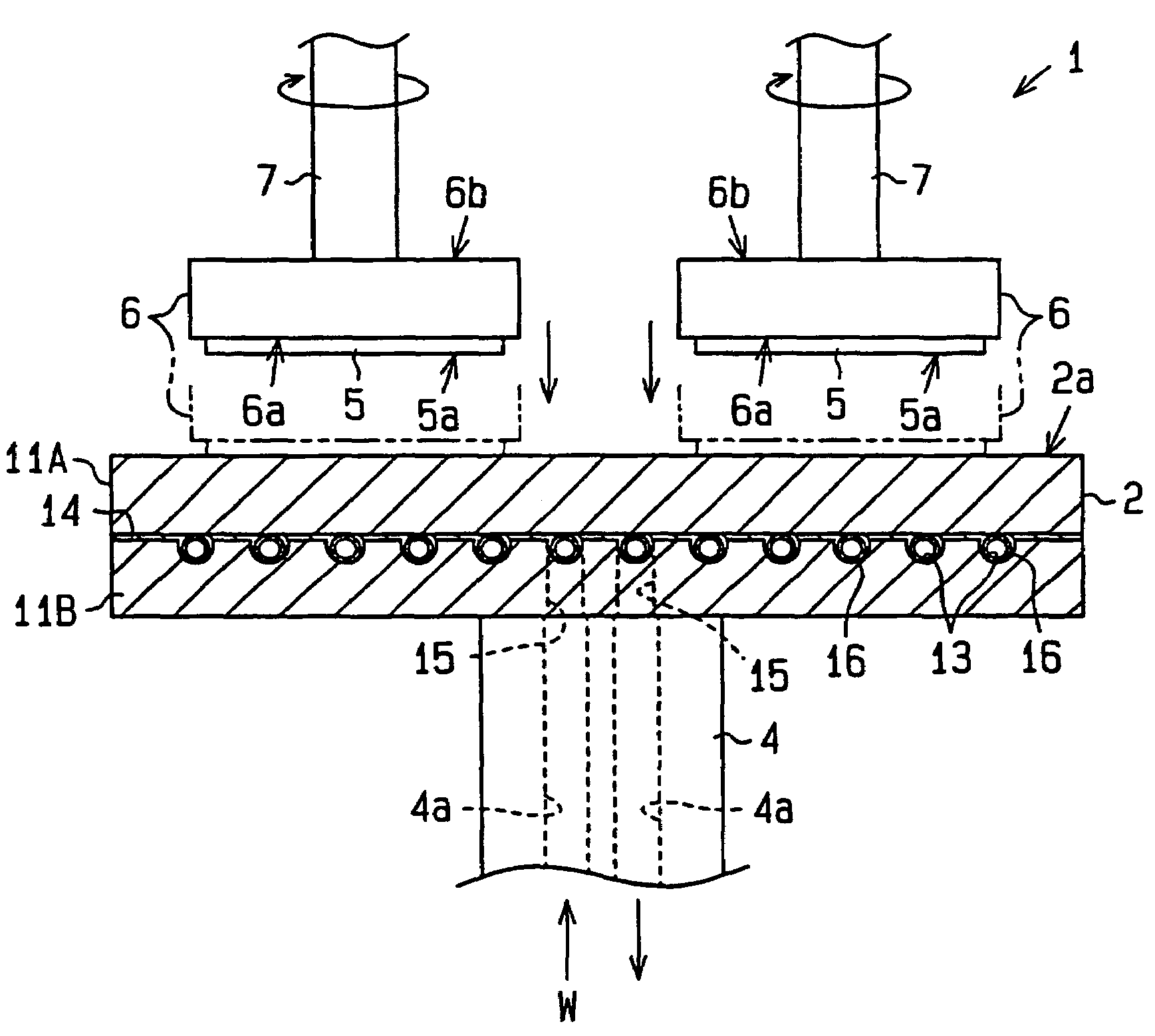
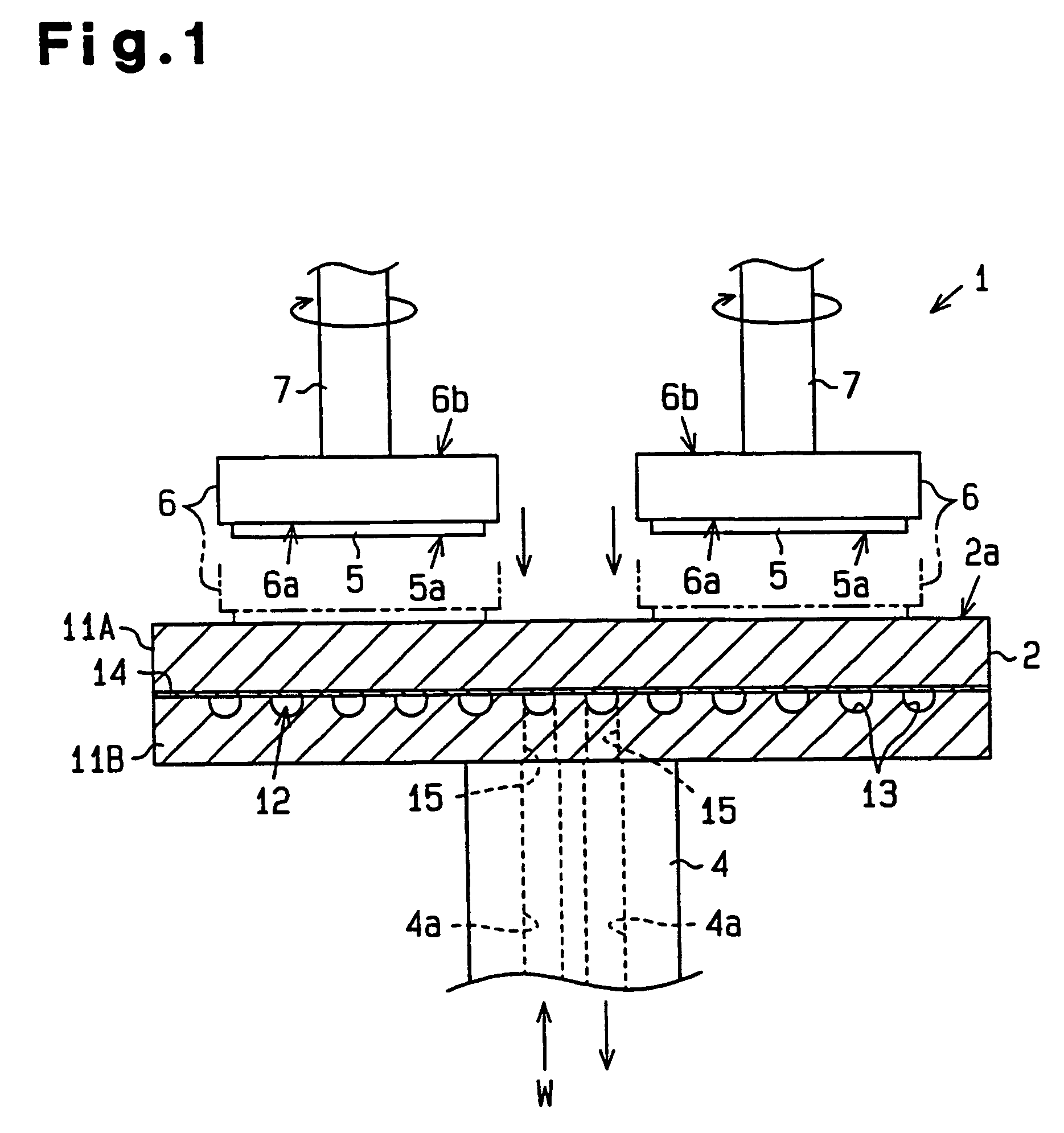
[0033]A wafer polishing apparatus 1 of the first embodiment will now be described in detail with reference to FIGS. 1 and 2. FIG. 1 schematically shows the wafer polishing apparatus 1 of the first embodiment. The wafer polishing apparatus 1 includes a disk-like table 2. A polishing surface 2a, on which a semiconductor wafer 5 is polished, is defined on the upper side of the table 2. A polishing cloth (not shown) is applied to the polishing surface 2a. In the first embodiment, a cooling jacket is not employed, and the table 2 is horizontally and directly secured to an upper end of a cylindrical rotary shaft 4. Thus, when the rotary shaft 4 is rotated, the table 2 rotates integrally with the rotary shaft 4.

[0034]As shown in FIG. 1, the wafer polishing apparatus 1 includes a plurality of wafer holding plates 6 (for the sake of brevity, only two are shown in FIG. 1). Each plate 6 is formed of, for example, glass, ceramic such as alumina, or metal such as stainless steel. A pusher rod 7 ...

referential example 1-1

[0049]In referential example 1-1, “beta random (trade name)”, product of IBIDEN KABUSHIKI KAISHA, was used as silicon carbide powder that contained 94.6 weight percent of β type crystals. The average crystal particle diameter of this powder was 1.3 micrometers. The powder contained 1.5 weight percent of boron and 3.6 weight percent of free carbon.

[0050]First, 5 weight parts of polyvinyl alcohol and 300 weight parts of water were added to 100 weight parts of the silicon carbide powder. The mixture was then stirred in a ball mill for five hours to obtain a uniform mixture. The mixture was dried for a predetermined time to remove a certain amount of moisture from the mixture. An appropriate amount of the dry mixture was then sampled and granulated. Next, the granules of the dry mixture were subjected to molding with metal press dies at a pressure of 50 kg / cm2. The density of the resulting molded body was 1.2 g / cm3.

[0051]Subsequently, the molded body was placed in a graphite crucible se...

referential example 1-2

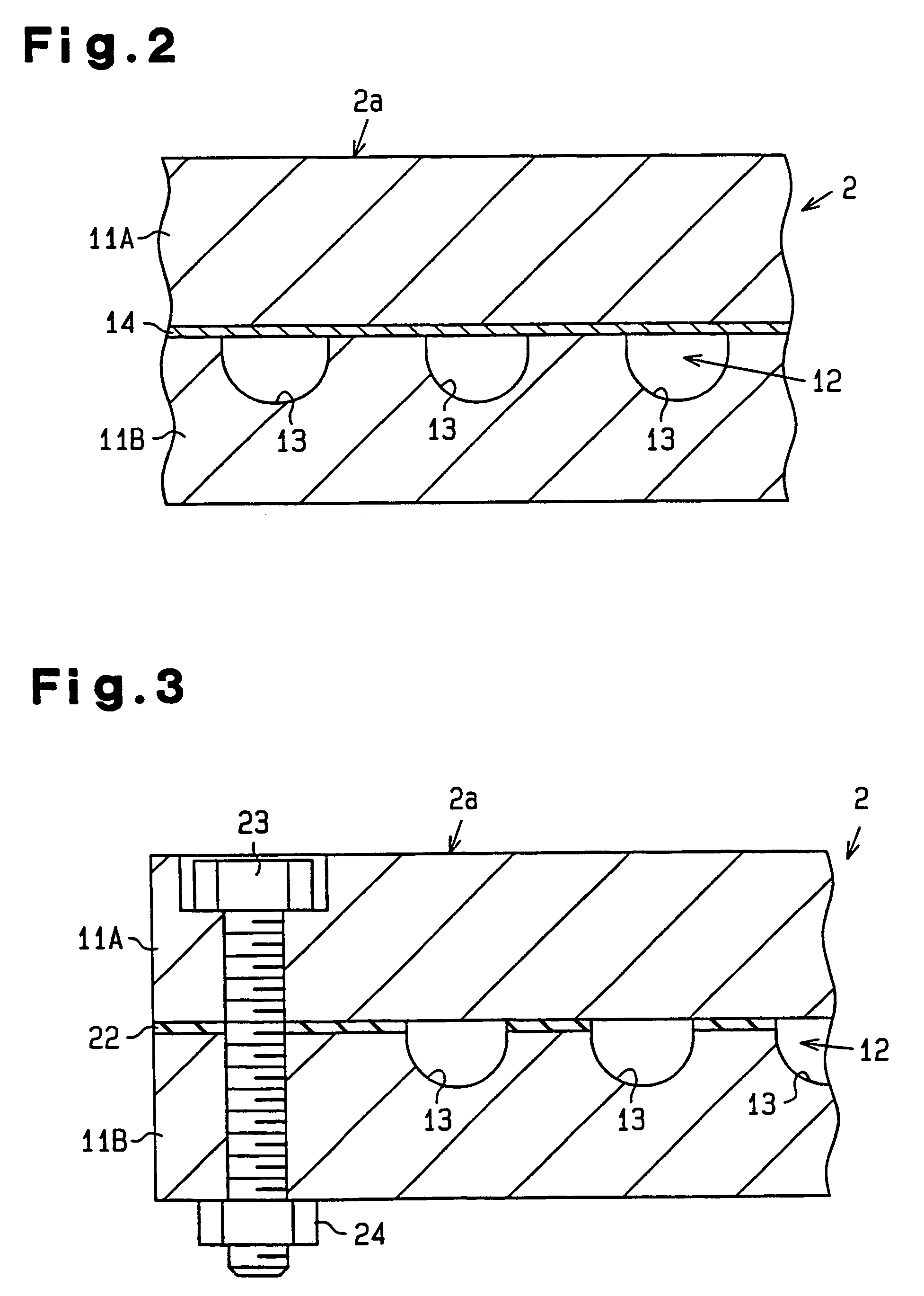
[0055]In referential example 1-2, a type silicon carbide powder (more specifically, “OY15 (trade name)”, product of YAKUSHIMA DENKO KABUSHIKI KAISHA) was employed in lieu of the β type. The density of each resulting base 11A, 11B was 3.1 g / cm3. The heat conductivity of each base 11A, 11B was 125 W / m·K. Each base 11A, 11B contained 0.4 weight percent of boron and 1.8 weight percent of free carbon. The heat conductivity of the bases 11A, 11B in referential example 1-1, in which the β type powder was the starting material, was approximately 20 percent higher than that of referential example 1-2.

[0056]After the table 2 was obtained through the same procedure as referential example 1-1, the table 2 was installed in the various types of apparatuses 1 to polish the semiconductor wafers 5 of different dimensions. Accordingly, substantially the same advantageous results as those of referential example 1-1 were obtained.

Conclusion

[0057]The first embodiment has the following advantages.

[0058](...


PUM

PropertyMeasurementUnit
densityaaaaaaaaaa
thicknessaaaaaaaaaa
thicknessaaaaaaaaaa

Abstract

A table for a wafer polishing apparatus having superior heat-resistant, anti-thermal-shock, and anti-abrasion characteristics and capable of increasing the diameter of a semiconductor wafer while improving the quality of the wafer. The table (2) includes a plurality of superimposed bases (11) each of which is formed of silicide ceramic or carbide ceramic. The bases (11) are joined together by an adhesive layer (14). A fluid passage (12) is formed in a joining interface between the bases (11).

Description

[0001]The present invention relates to a table of a semiconductor wafer polishing apparatus, a method for polishing semiconductor wafers with the polishing apparatus, and a method for manufacturing a semiconductor wafer with the polishing apparatus.BACKGROUND OF THE INVENTION[0002]These days, most electric products employ a semiconductor device that includes a fine conductive circuit formed on a silicone chip. Generally, the semiconductor device is fabricated using a monocrystal silicon ingot as a starting material in accordance with the following procedure.[0003]First, the ingot is sliced into thin pieces. The pieces are then polished in a lapping step and a polishing step to obtain bare wafers. The bare wafers include mirror surfaces and are thus referred to as mirror wafers. Also, if the bare wafers are obtained in an epitaxial growth layer forming step after the lapping step and before the polishing step, the bare wafers are particularly referred to as epitaxial wafers.[0004]In ...

Claims


Application Information

Patent Timeline
Patent Type & Authority Patents(United States)
IPC IPC(8): B24B1/00B24B37/015B24B37/12B24B37/14B24B37/16B24B41/047B24B49/14
CPCB24B37/015B24B37/12B24B55/02B24B37/16B24B41/047B24B37/14
Inventor OKUDA, YUJIJIMBO, NAOYUKIMAJIMA, KAZUTAKATSUJI, MASAHIROTAKAGI, HIDEKIISHIKAWA, SHIGEHARUYASUDA, HIROYUKI
Owner IBIDEN CO LTD
Why Eureka
Try Eureka