Film forming method for depositing a plurality of high-k dielectric films

a film forming method and dielectric film technology, applied in the direction of coatings, transistors, chemical vapor deposition coatings, etc., can solve the problems of large change in the capacity of the capacitor structure accompanied by the change in applied voltage, and achieve the effect of suppressing the change in capacity and low leakage curren

Active Publication Date: 2006-05-09
TOKYO ELECTRON LTD
View PDF6 Cites 5 Cited by
  • Summary
  • Abstract
  • Description
  • Claims
  • Application Information

AI Technical Summary

Benefits of technology

[0010]The object of the present invention is to provide a capacitor structure that achieves suppression of increase in the leakage current accompanied with increase in applied operation voltage and suppression of change in capacity due to the change in applied voltage, without excessive increase in the thickness of the dielectric layer.
[0013]According to the present invention, as the silicon-free high dielectric film and said at least one layer of silicon-containing high dielectric film are interposed between a lower electrode film and an upper electrode film, low leak current is achieved even when the applied voltage in operation is high, and suppression of change in the capacity accompanied with change in the applied voltage is achieved, without excessive increase in the thickness of dielectric layers.

Problems solved by technology

However, in the aforementioned conventional MIM structure, although leakage current is sufficiently low if low operation voltage such as about ±1V is applied thereto, leakage current is considerably high if high operation voltage such as about ±5V is applied thereto.
In addition, a slight change in a capacity of the capacitor structure accompanied with a change of an applied voltage is inherently inevitable, but with aforesaid conventional MIM structure, change in the capacity of the capacitor structure accompanied with change in applied voltage is considerably large.

Method used


Image

  • Film forming method for depositing a plurality of high-k dielectric films
  • Film forming method for depositing a plurality of high-k dielectric films
  • Film forming method for depositing a plurality of high-k dielectric films

Examples


first embodiment

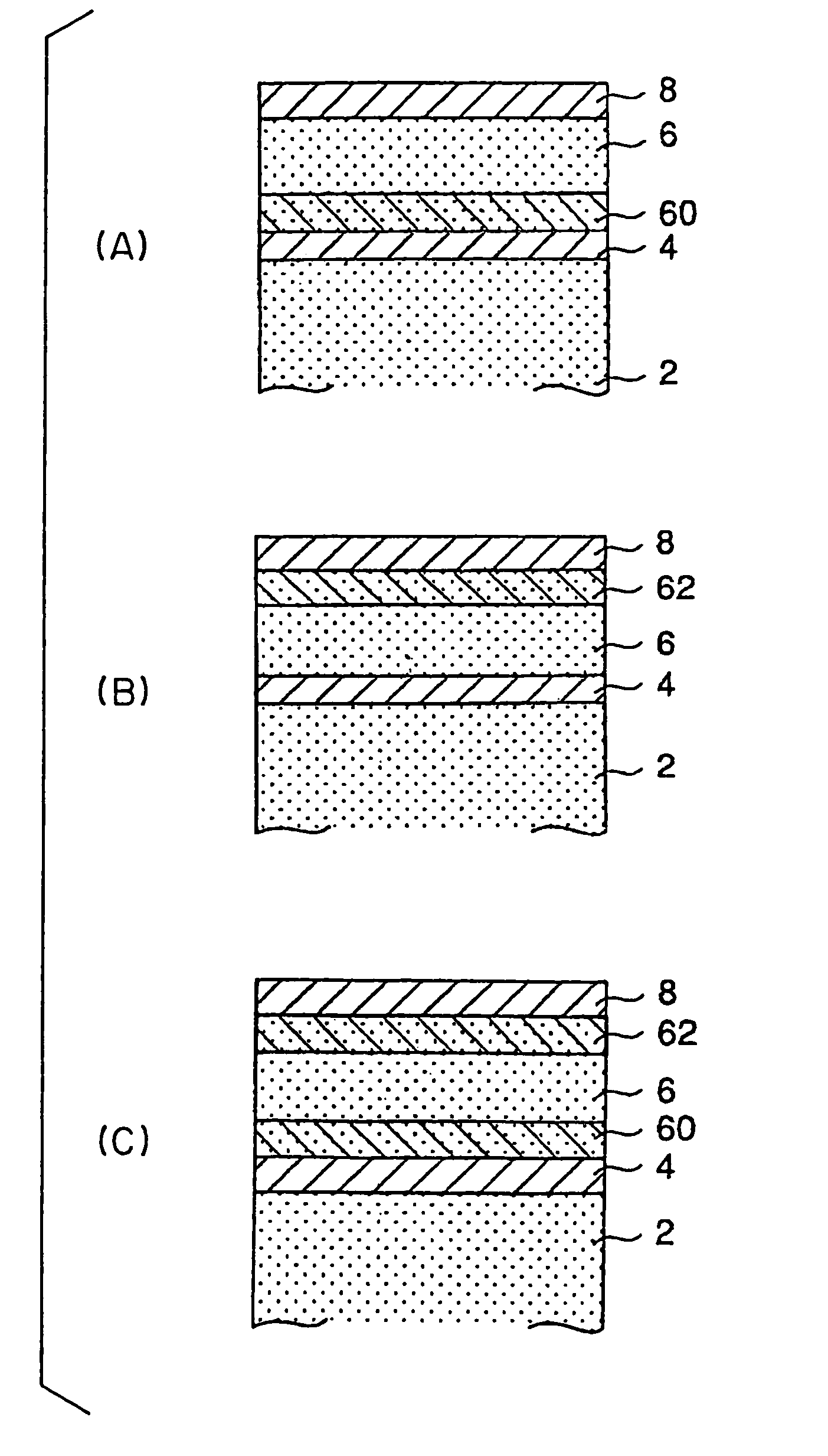
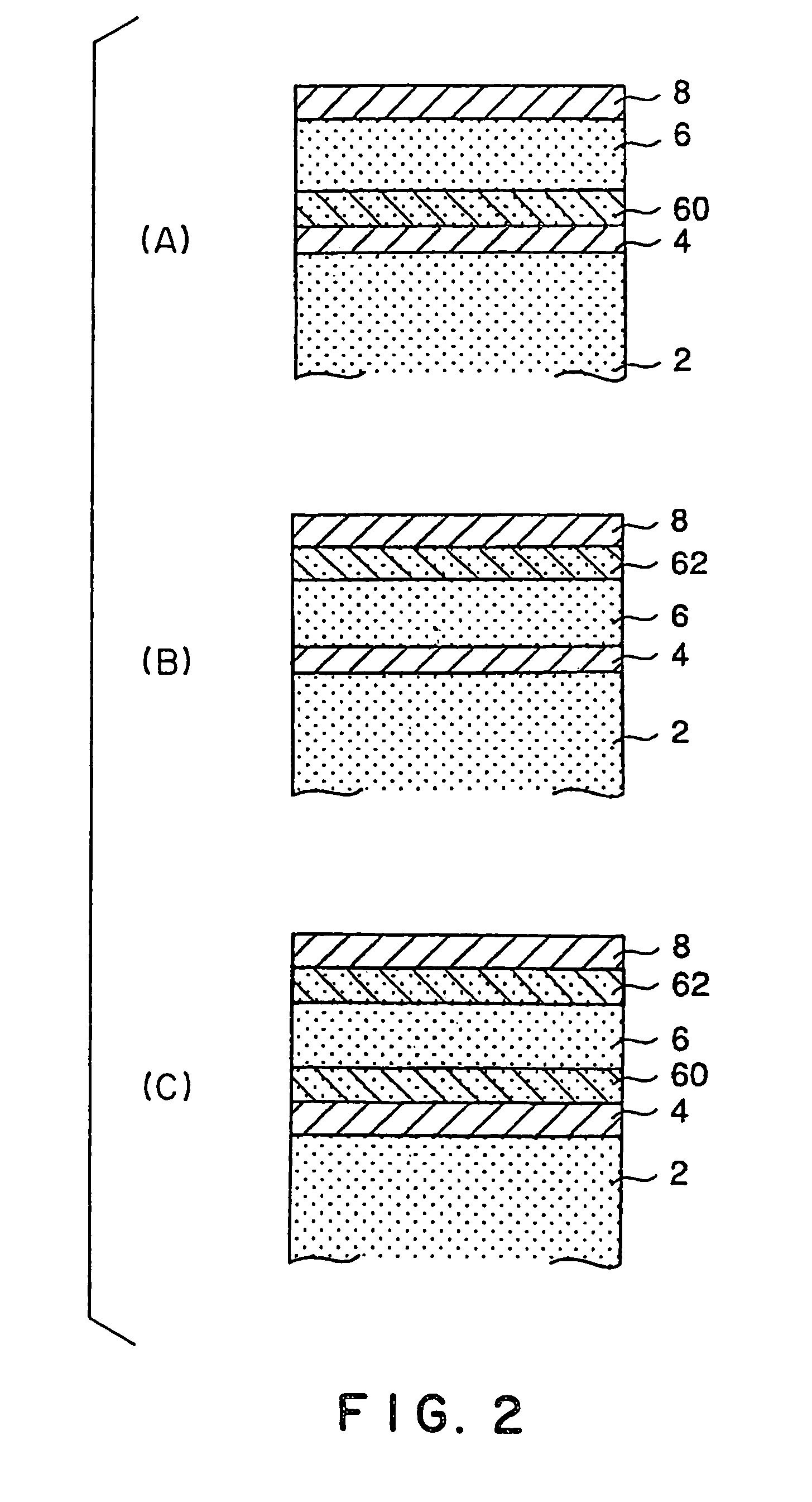
[0042]FIG. 2 shows embodiments of the capacitor structure according to the present invention. In FIG. 2, the same elements as shown in FIG. 6 are designated by the same reference numerals. In the first embodiment shown in FIG. 2(A), a lower electrode 4, a silicon-containing high dielectric film 60 of hafnium silicate, a silicon-free high dielectric film (tantalum oxide film) 6 of tantalum oxide, and an upper electrode 8 are stacked in that order on a surface of a semiconductor wafer 2 formed of a silicon substrate. The lower electrode 4 and the upper electrode 8 are formed by means of a sputtering apparatus which is separated from the film forming apparatus.

second embodiment

[0043]In the second embodiment shown in FIG. 2(B), a lower electrode 4, a silicon-free high dielectric film (tantalum oxide film) 6 of tantalum oxide, a silicon-containing high dielectric film 62 of hafnium silicate, and an upper electrode 8 are stacked in that order on a surface of a semiconductor wafer 2.

third embodiment

[0044]In the third embodiment shown in FIG. 2(C), a lower electrode 4, a first silicon-containing high dielectric film 60 of hafnium silicate, a silicon-free high dielectric film (tantalum oxide film) 6 of tantalum oxide, a second silicon-containing high dielectric film 62 of hafnium silicate, and an upper electrode 8 are stacked in that order on a surface of a semiconductor wafer 2.

[0045]A method of forming the high dielectric film will be described below.

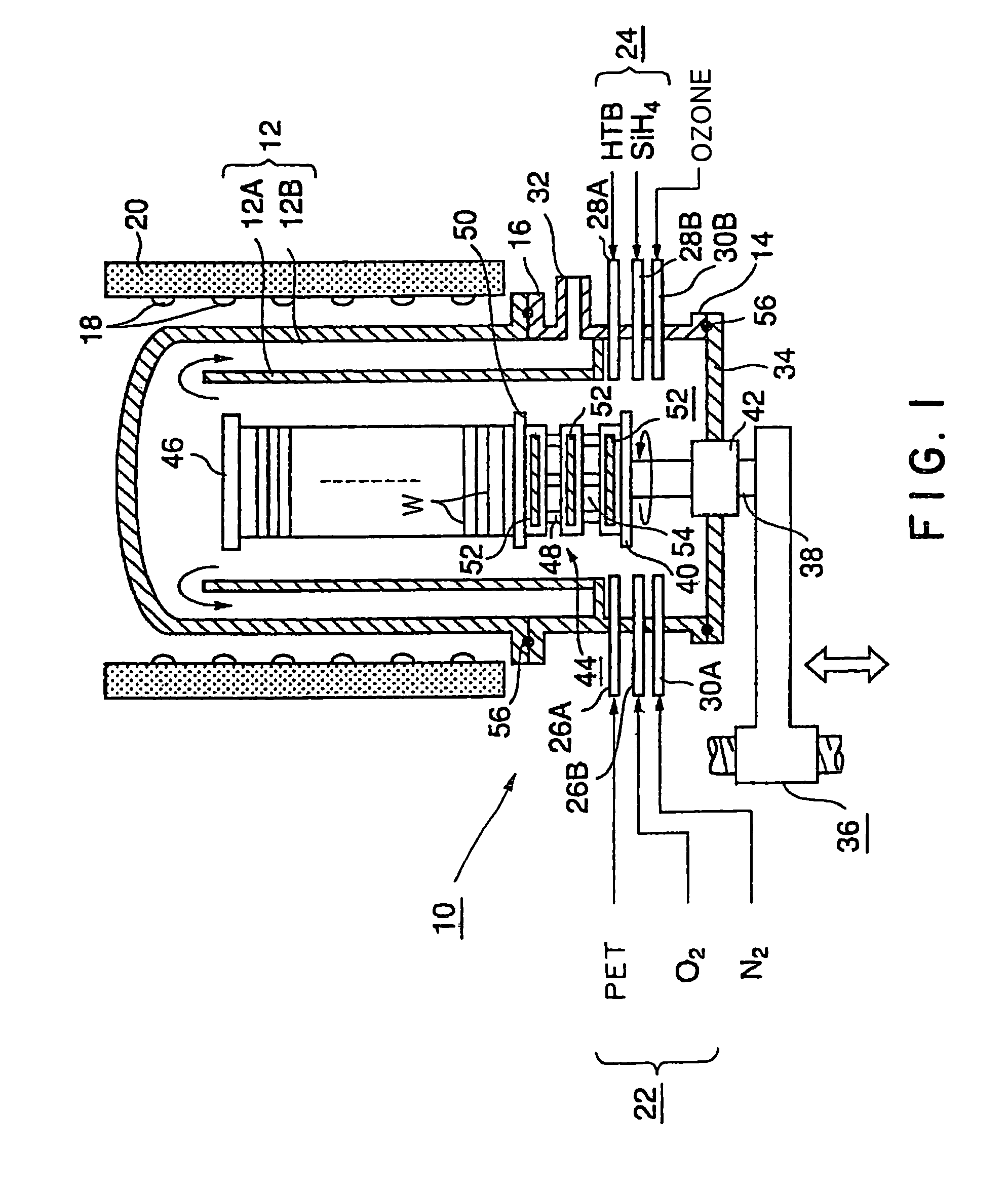
[0046]In an unloading condition where the cap 34 is lowered, a plurality of unprocessed semiconductor wafers W are placed on the wafer boat 46 at predetermined intervals in multistage. The wafer boat 46 holds, for example, about 50 to 100 pieces of 8-inch wafers arranged thereon. The lower electrode 4 shown in FIG. 2 has been already deposited on each semiconductor wafer W by sputtering process performed under a process temperature of room temperature to about 200° C. by means of a sputtering apparatus. The lower electrode 4 has b...


PUM

PropertyMeasurementUnit
thicknessaaaaaaaaaa
thicknessaaaaaaaaaa
temperatureaaaaaaaaaa

Abstract

In a capacitor of an MIM (Metal-Insulator-Metal) structure, a silicon-containing high dielectric film (e.g., a hafnium silicate film) containing a silicon atom, as well as a silicon-free high dielectric film (e.g., a tantalum oxide film) containing no silicon atom is interposed between a lower electrode film and an upper electrode film which are made of metal or metal compound. By adding the silicon-containing high dielectric film, a leak current can be suppressed and the change in capacitor capacity accompanied with the change in applied voltage can be reduced.

Description

TECHNICAL FIELD[0001]The present invention relates to a capacitor structure, a film forming method, and a film forming apparatus.BACKGROUND ART[0002]In manufacturing a semiconductor device, a semiconductor wafer is repeatedly subjected to a film forming process and a pattern etching process, in general. Design rules are becoming stricter every year in accordance with a recent increase in density and integration of semiconductor devices. For example, a very thin oxide film such as an insulator film of a capacitor structure is required to be much thinner, and have a higher insulation performance as well.[0003]Although silicon oxide film and a silicon nitride film may be used as such insulation film, the recent trend is to use a metal oxide film having a higher insulation performance, such as tantalum oxide film (Ta2O5). The metal oxide film has a reliable insulation performance even if the film thickness is small.[0004]When forming a tantalum oxide film, pentaethoxytantalum (Ta(OC2H5)...

Claims


Application Information

Patent Timeline
Patent Type & Authority Patents(United States)
IPC IPC(8): H01L21/8238C23C16/42H01L21/02H01L21/31H01L21/316H01L21/822H01L27/04
CPCH01L28/40H01L21/31612H01L21/31637H01L28/56H01L21/31645H01L21/02164H01L21/02183H01L21/02181
Inventor MOROZUMI, YUICHIROHASEBE, KAZUHIDENAKAJIMA, SHIGERUFURUYA, HARUHIKOCHOI, DONG-KYUNUMEHARA, TAKAHITOHARADA, KATSUSHIGEFUJIWARA, TOMONORIFUJITA, HIROTAKE
Owner TOKYO ELECTRON LTD
Why Eureka
Try Eureka