Method for determining metal work function by formation of Schottky diodes with shadow mask

a diode and shadow mask technology, applied in the field of metal gate work function determination, can solve the problems of reducing the controllability of the gate, the metal gate cannot withstand the higher temperature and oxidation ambient, and the polysilicon gate electrod

Inactive Publication Date: 2006-05-16
GLOBALFOUNDRIES US INC
View PDF5 Cites 3 Cited by
  • Summary
  • Abstract
  • Description
  • Claims
  • Application Information

AI Technical Summary

Benefits of technology

[0008]There is a need for a method of screening potential m

Problems solved by technology

However, polysilicon gate electrodes have certain disadvantages.
However, metal gates cannot withstand the higher temperatures and oxidation ambient that can be withstood by conventional polysilicon gate electrodes.
The use of metal, however, as the gate material on the silicon substrate normally undesirably changes the work function in comparison to polysilicon gates.
This reduces the con

Method used


Image

  • Method for determining metal work function by formation of Schottky diodes with shadow mask
  • Method for determining metal work function by formation of Schottky diodes with shadow mask
  • Method for determining metal work function by formation of Schottky diodes with shadow mask

Examples


Embodiment Construction

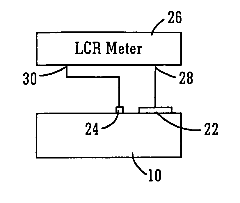
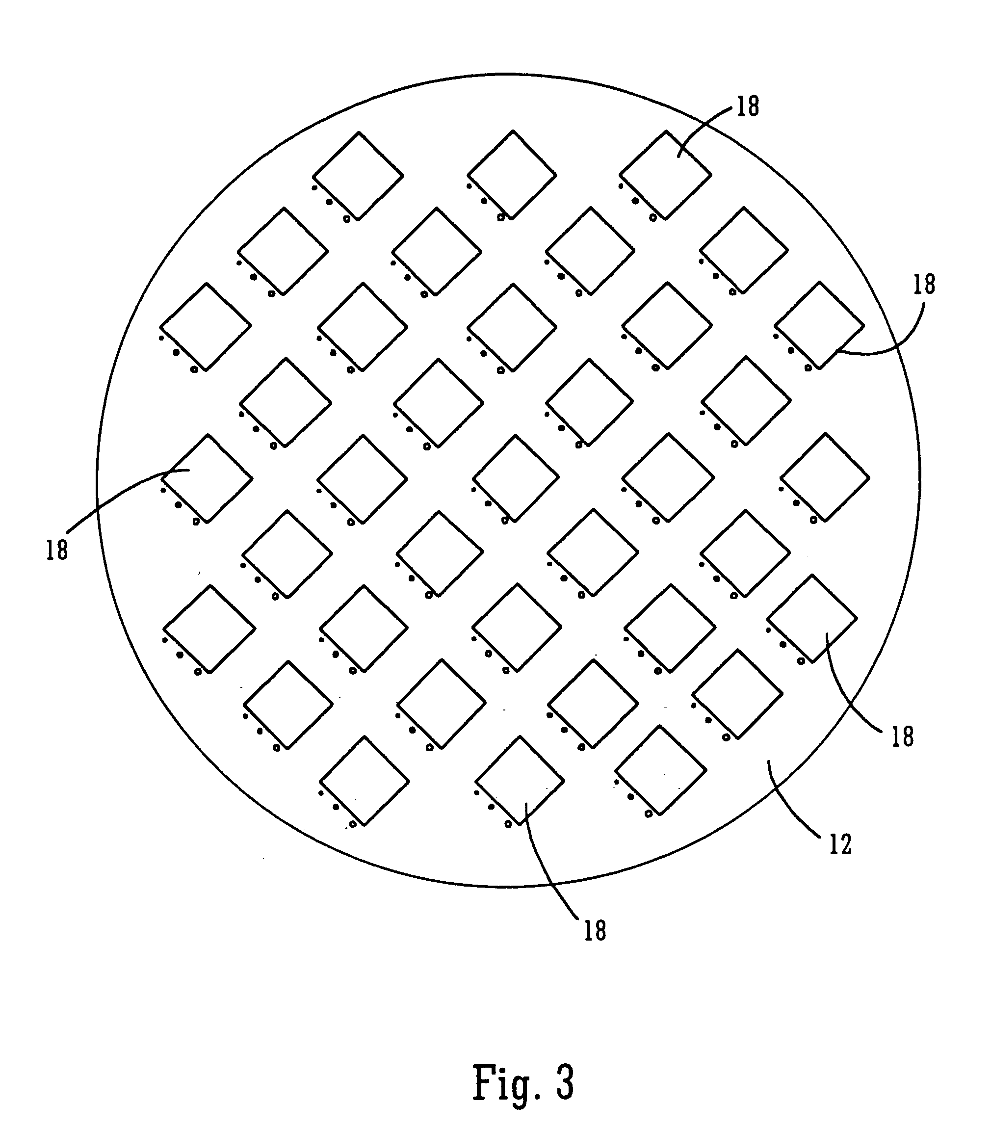
[0018]The present invention addresses and solves problems related to the screening of potential metal gate materials for use in semiconductor devices. In particular, the traditional methods of forming Schottky diodes to measure metal work function employed conventional lithography, metal deposition and etch processing steps. The present invention avoids such steps by forming a metal deposition on blanket silicon wafers with a metal gate material whose work function is to be determined. This is accomplished by the use of a shadow mask having specified repeating patterns. The metal-on-silicon formed by the deposition of metal through the holes in the shadow mask create a Schottky diode. By measurement of the capacitance-voltage curve of the Schottky diode, the work function of the metal can be determined.

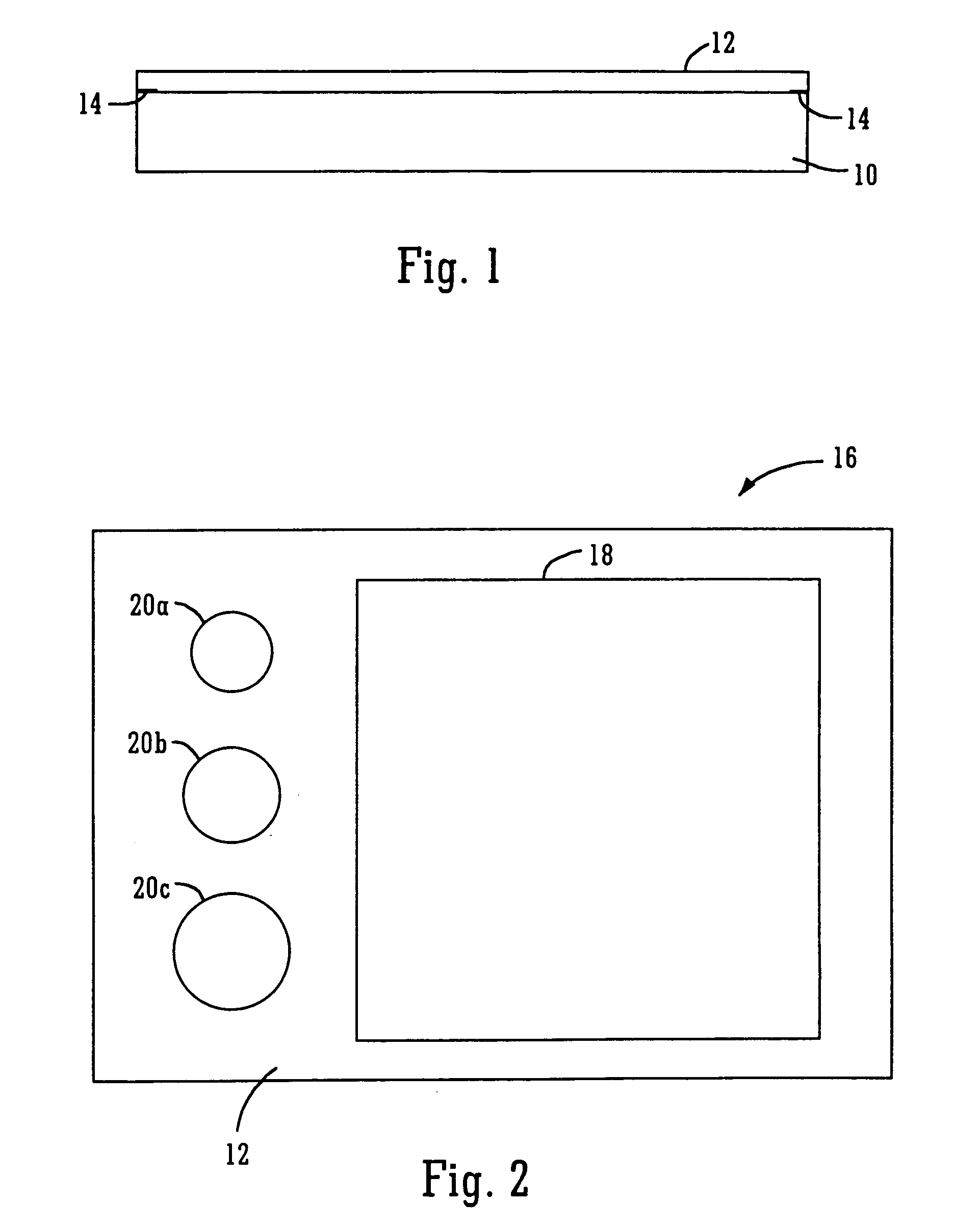
[0019]FIG. 1 schematically depicts an arrangement for preparing a Schottky diode to determine a metal work function in accordance with embodiments of the present invention. A silicon ...


PUM


Abstract

A method of determining a work function of a metal to be used as a metal gate material provides a metal-on-silicon (MS) Schottky diode on a silicon substrate. The MS Schottky diode is formed by deposition of the metal in a single step deposition through a shadow mask that is secured on the silicon substrate.

Description

FIELD OF THE INVENTION[0001]The present invention relates to the field of semiconductor processing, and more particularly, to the determination of the work function of metal gates.BACKGROUND OF THE INVENTION[0002]In the integrated circuit (IC) industry, metal-oxide-semiconductor (MOS) transistors have typically been formed utilizing polysilicon gate electrodes. Polysilicon material has been preferred for use as a MOS gate electrode due to its thermal resistive properties (i.e., polysilicon can better withstand subsequent high temperature processing). Polysilicon's robustness during high temperature processing allows polysilicon to be annealed at high temperatures along with the source and drain regions. Furthermore, polysilicon's ability to block the ion implantation of doped atoms into a channel region is advantageous. Due to the ion implantation blocking potential of polysilicon, polysilicon allows for the easy formation of self-aligned source and drain structures after gate patte...

Claims


Application Information

Patent Timeline
IPC IPC(8): H01L21/00
CPCH01L29/66143G01R31/2831
Inventor PAN, JAMES N.WOO, CHRISTY MEI-CHU
Owner GLOBALFOUNDRIES US INC
Why Eureka
Try Eureka