

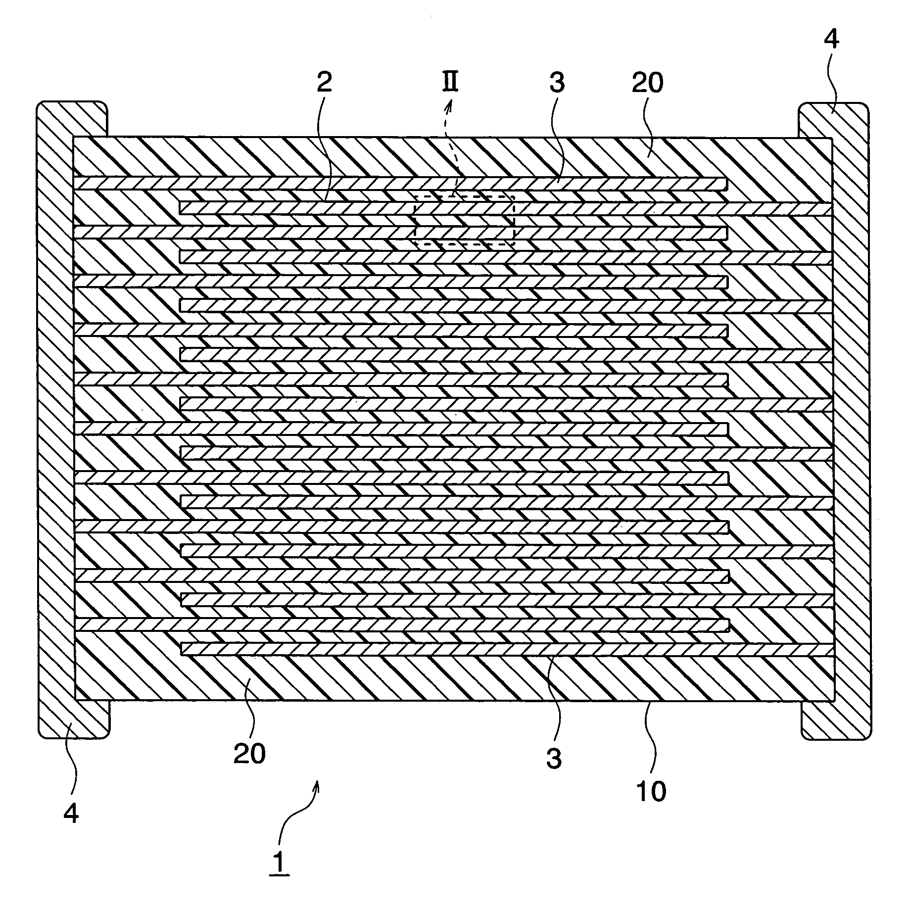
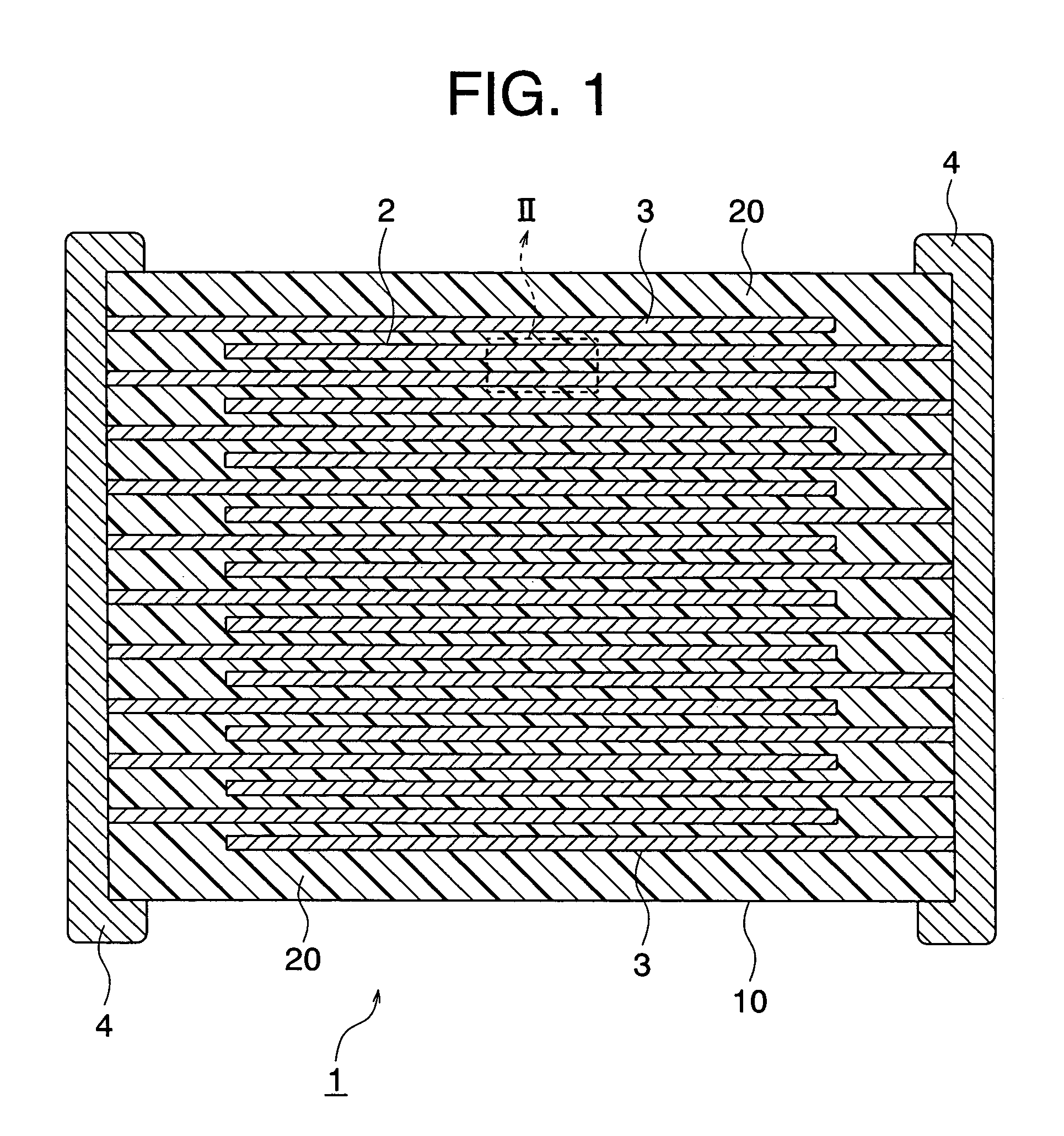
Multilayer ceramic capacitor
a multi-layer ceramic and capacitor technology, applied in the field of multi-layer ceramic capacitors, can solve the problems of deterioration of bias characteristics and reliability, difficulty in solving problems, and insufficient improvement of bias characteristics, so as to and improve tc bias characteristics.
- Summary
- Abstract
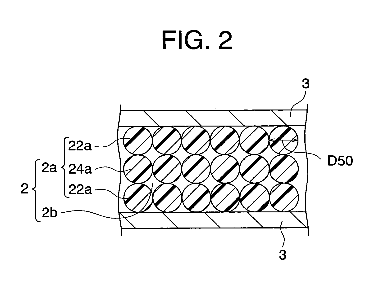
- Description
- Claims
- Application Information
AI Technical Summary
Benefits of technology
Problems solved by technology
Method used
Image

Examples
example 1
Production of Dielectric Layer Paste
[0126]First, a dielectric material, a polyvinyl butyral (PVB) resin as a binder, diotycle phthalate (DOP) as a plasticizer, and ethanol as a solvent were prepared.
[0127]The dielectric material was produced by wet mixing barium titanate having an average particle diameter of about 0.2 μm as a main component material (specifically, barium titanate expressed by a composition formula of (BaO)m.TiO2, wherein the mole ratio m is 1.005), 0.2 mole % of MnC, 0.5 mole % of MgO, 0.3 mole % of V2C5, 2 mole % of Y2O3, 3 mole % of CaCO3, 3 mole % of BaCO3 and 3 mole % of SiO2 as suboopponents for 16 hours by a ball-mill and dried.
[0128]Next, 10 wt % of a binder, 5 wt % of a plasticizer and 150 wt % of a solvent with respeat to the dielectric material were weighed, kneaded by a ball-mill and made to be a slurry, so that a dielectric layer paste was obtained.
[0129]Production of Internal Electrode Layer Paste
[0130]Ni particles having an average particle diameter o...
example 2
[0161]Other than changing a thickness of the interlayer dielectric layer 2 to 1.9 μm, 1.7 μm, 1.5 μm, 1.3 μm and 0.9 μm, capacitor samples were produced in the same way as in the example 1, and the same evaluation was made. As a result, the same results were obtained.
PUM
| Property | Measurement | Unit |
|---|---|---|
| thickness | aaaaa | aaaaa |
| thickness | aaaaa | aaaaa |
| thickness | aaaaa | aaaaa |
Abstract
Description
Claims
Application Information