Semiconductor chip mounting wiring board, manufacturing method for same, and semiconductor module

a semiconductor chip and mounting board technology, applied in the direction of printed circuit manufacturing, conductive pattern formation, printed electric component incorporation, etc., can solve the problems of poor electrical connection and reliability of the wiring board, the wiring board cannot be easily stacked on each other, and the wires led out of the semiconductor chip cannot be connected to the stack of the wiring board

Inactive Publication Date: 2006-05-23
IBIDEN CO LTD
View PDF13 Cites 42 Cited by
  • Summary
  • Abstract
  • Description
  • Claims
  • Application Information

AI Technical Summary

Benefits of technology

[0108]The semiconductor chip mounting wiring board according to the present invention is used to produce a semiconductor module by stacking and hot-pressing of the wiring boards each having a semiconductor chip such as an IC chip or the like mounted on conductive bumps and interlayer members each having an opening to receive the semiconductor chip, alternately on each other. The semiconductor module thus produced can be of a high mounting density and low profile type permitting a quick information transmission between the semiconductor chips, and is highly connection-reliable.

Problems solved by technology

So, wiring boards of this type cannot easily be stacked on each other.
Even if they are stacked on each other, it is very difficult to connect the wires led out of the semiconductor chips to the stack of the wiring boards because the wiring board having the semiconductor chip buried in the substrate thereof is basically different in structure from the wiring board to be stacked on the former wiring board.
Therefore, even if such ceramic substrates are stacked on each other, they are likely to be delaminated from each other, which causes the electrical connection and reliability of the wiring boards to be poor.
These conventional techniques need many manufacturing steps, which adds to the processing costs.

Method used


Image

  • Semiconductor chip mounting wiring board, manufacturing method for same, and semiconductor module
  • Semiconductor chip mounting wiring board, manufacturing method for same, and semiconductor module
  • Semiconductor chip mounting wiring board, manufacturing method for same, and semiconductor module

Examples


first embodiment

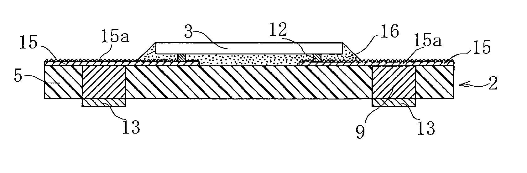
[0109]the semiconductor chip mounting wiring board according to the present invention includes an insulating resin substrate having defined nearly in the center on one side thereof an area in which a semiconductor chip is to be mounted, a plurality of conductive bumps (will be referred to as “first conductive bump” hereunder) formed around the mounting area to mount a plurality of semiconductor chips, respectively, and a wiring pattern electrically connected to the first conductive bumps and extending from the mounting area toward the periphery of the insulating resin substrate.

[0110]Also, openings are formed which lead from the other side of the insulating resin substrate to the wiring pattern, a filled viahole is formed from a conductive substance filled in each of the openings, and an interconnecting conductive bump (will be referred to as “second conductive bumps” hereunder) is formed just above each viahole, respectively, and electrically connected to each interlayer member.

[01...

embodiment 1

[0264

[0265](1) A glass fabric was impregnated with epoxy resin to prepare a B-stage prepreg. A copper foil was attached to the prepreg. They were pressed while being heated to prepare a one-side copper-clad laminate 4. This one-side copper-clad laminate 4 was used as the starting material for the semiconductor chip mounting wiring board 2. The insulating resin substrate 5 was 75 μm thick and copper foil 12 was 12 μm thick (as shown in FIG. 3(a)).

[0266](2) A PET film 7 having a thickness of 22 μm was attached to the side of the insulating resin substrate 5 opposite to the side to which the copper foil 6 was attached. The PET film 7 comprised an adhesive layer of 10 μm in thickness and PET film base of 12 μm in thickness.

[0267](3) Next, a pulse oscillation type carbon dioxide gas laser machine was used to irradiate a laser beam from above the PET film 7 to the insulating resin substrate 5 under the following laser beam machining conditions to form the opening 8 in which the viahole wa...

embodiment 2

[0299

[0300](1) By conducting processes as in the steps (1) to (9) for the embodiment 1, a mounting wiring board 2 having a semiconductor chip 3 mounted thereon was prepared (as shown in FIGS. 3(a) to 4(e)).

[0301](2) Next, a glass fabric was impregnated with epoxy resin. The glass fabric thus processed was heated to a semi-hardened state, and then shaped to be a plate which was a prepreg of 150 μm in thickness. The prepreg was used as the insulating resin substrate 21 for the interlayer member 20 (as shown in FIG. 8(a)).

[0302]A protective film 23 of 23 μm in thickness was attached to either side of the insulating resin substrate 21 formed from the prepreg (as shown in FIG. 8(b)). A pulse oscillation type carbon dioxide gas laser machine was used to irradiate a laser beam from below the insulating resin substrate 21 under the following conditions to form a truncated-conical through-hole 24 having a diameter of 250 μm at the lower opening and a diameter of 100 μm at the upper opening (...


PUM

PropertyMeasurementUnit
melting pointsaaaaaaaaaa
thickaaaaaaaaaa
thickaaaaaaaaaa

Abstract

A semiconductor chip mounting wiring board 2 includes an insulating resin substrate 5, a first conductive bump 12 formed on one side of the insulative resin substrate 5 to mount a semiconductor chip 3, a wiring pattern 15 extending from the first conductive bump 12 toward the periphery of the insulating resin substrate 5, a filled viahole 9 leading from the other side of the insulating resin substrate 5 to the wiring pattern 15, and a second conductive bump 13, or a conductive pad 19, positioned just above the filled viahole 9 and electrically connected to the viahole 9. A semiconductor module is produced by mounting the semiconductor chip 3 in advance on the first conductive bump 12 on the semiconductor chip mounting wiring board 2 and stacking a plurality of the wiring boards 2 and interlayer members 20 each having an opening 27 to receive the semiconductor chip 3 and a conductive post 26 or conductive pad connected to the second conductive bump 13 of the wiring board 2 alternately on each other with an adhesive applied between them, placing another interconnecting circuit board such as an I / O wiring board 30 or the like on an outermost layer, and by applying hot-pressing to the stack. The semiconductor module thus produced has a high connection reliability and can be designed for a high mounting density and a lower profile.

Description

FIELD OF THE INVENTION[0001]The present invention relates to a wiring board suitable for mounting semiconductor chips such as IC chip and the like on a wiring pattern provided on an insulating resin substrate, a method of manufacturing the wiring board, and a semiconductor module formed by stacking wiring boards having semiconductor chips mounted thereon and interlayer members alternately on each other.BACKGROUND ART[0002]To meet the demands for improved mounting densities and functionality of printed wiring boards, techniques have recently been proposed to bury each of semiconductor chips in a substrate.[0003]As one typical example of such techniques, a package having each semiconductor chip buried in a ceramic substrate is known from the disclosure in JP H10-256429 A. The package has a BGA (ball grid array) structure in which a semiconductor chip is buried in a concavity formed in the ceramic substrate and connected to a conductive circuit formed in the ceramic substrate by the fl...

Claims


Application Information

Patent Timeline
Patent Type & Authority Patents(United States)
IPC IPC(8): H05K1/11H05K1/00H01L21/98H01L23/12H01L25/065
CPCH01L23/49811H01L23/49833H01L24/32H01L25/0657H01L25/50H01L24/29H01L2224/16225H01L2224/27013H01L2224/48091H01L2224/48247H01L2224/73204H01L2224/83051H01L2224/83101H01L2225/0651H01L2225/06517H01L2225/0652H01L2225/06541H01L2225/06551H01L2225/06555H01L2225/06572H01L2225/06586H01L2225/06589H01L2924/01002H01L2924/01005H01L2924/01013H01L2924/01015H01L2924/01025H01L2924/01027H01L2924/01029H01L2924/0103H01L2924/01033H01L2924/01047H01L2924/01049H01L2924/0105H01L2924/01078H01L2924/01079H01L2924/01082H01L2924/14H01L2924/15311H01L2924/1532H01L2924/15331H01L2924/18301H01L2924/30107H01L24/48H01L2224/32225H01L2924/01006H01L2924/01019H01L2924/01023H01L2924/01087H01L2924/0132H01L2224/32245H01L2224/73265H01L2224/45147H01L2924/3511H01L2924/1579H01L2224/29111H01L2224/2919Y10T29/49156Y10T29/4913Y10T29/49155H01L2924/00014H01L2924/00H01L2924/3512H01L2924/00012H01L24/45H01L24/73H01L2224/05001H01L2224/05023H01L2224/05568H01L2224/05573H01L2924/12042H01L2924/15787H01L2924/1627H01L2924/181H01L2224/05599
Inventor KARIYA, TAKASHINISHIKAWA, MASAYA
Owner IBIDEN CO LTD
Why Eureka
Try Eureka