Digital isolation system with hybrid circuit in ADC calibration loop

a digital isolation system and hybrid circuit technology, applied in the field of isolation systems, can solve the problems of transformer size, weight and cost, cost disadvantage, and analog signal communication through a transformer is subject to low frequency bandwidth limitations

Inactive Publication Date: 2006-05-23
SILICON LAB INC
View PDF234 Cites 76 Cited by
  • Summary
  • Abstract
  • Description
  • Claims
  • Application Information

AI Technical Summary

Problems solved by technology

However, analog signal communication through a transformer is subject to low frequency bandwidth limitations, as well as distortion caused by core nonlinearities.
Further disadvantages of transformers are their size, weight and cost.
However, two separate pulse transformers are disclosed for bidirectional communication with this technique, resulting in a cost disadvantage.
Another disadvantage of transformer coupling is that additional isolation elements, such as relays and opto-isolators, are typically required to transfer control signal information, such as phone line hookswitch control and ring detect, across the isolation barrier, further increasing the cost and size of transformer-based isolation solutions.
The disadvantage of this technique is that the analog communication, although differential, is not robust.
Mismatches in the differential components allow noise signals, which can capacitively couple into the isolation barrier, to easily corrupt both the amplitude and timing (or phase) of the analog modulated signal, resulting in unreliable communication across the barrier.
This scheme also requires separate isolation components for control signals, such as hookswitch control and ring detect, which increase the cost and complexity of the solution.
Furthermore, since capacitively coupled noise can cause timing (or phase) errors of voltage transitions in addition to amplitude errors, these modulation schemes remain sensitive to noise interference at the isolation barrier.
Consequently one disadvantage of this approach is that noise capacitively coupled at the isolation barrier can cause clock signal timing errors known as jitter, which corrupts the recovered analog signal and results in unreliable communication across the isolation barrier.
Reliable signal communication is further compromised by the sensitivity of the single ended signal transfer to voltages that exist between the isolated circuit sections.
Further disadvantages of the method described in this data sheet are the extra costs and board space associated with other required isolating elements, including a separate high voltage isolation capacitor for the clock signal, another separate isolation capacitor for bidirectional communication, and opto-isolators and relays for communicating control information across the isolation barrier.
As described, the modulation scheme encodes the signal information into on / off transitions of the LED at precise moments in time, thereby becoming susceptible to the same jitter (transition timing) sensitivity as the capacitive isolation amplifier modulation schemes.
In either case, no mechanism is provided for jitter insensitive communication of the ADC clock, which is required for reliable signal reconstruction, across the isolation barrier.
Some further disadvantages of optical isolation are that opto-isolators are typically more expensive than high voltage isolation capacitors, and they are unidirectional in nature, thereby requiring a plurality of opto-isolators to implement bidirectional communication.

Method used


Image

  • Digital isolation system with hybrid circuit in ADC calibration loop
  • Digital isolation system with hybrid circuit in ADC calibration loop
  • Digital isolation system with hybrid circuit in ADC calibration loop

Examples


Embodiment Construction

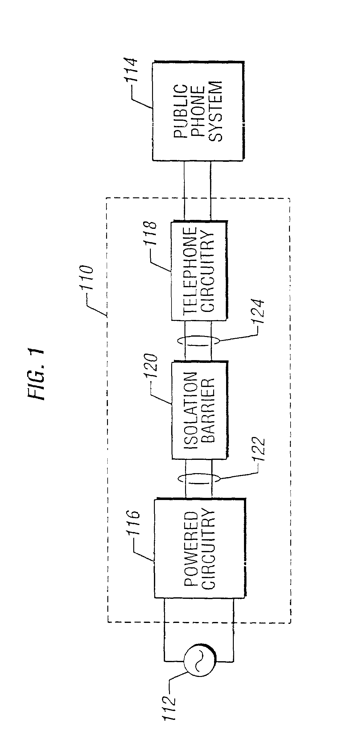
[0037]In order to provide a context for understanding this description, FIG. 1 illustrates a typical application for the present invention: a telephone that includes circuitry powered by a source external to the phone system. A basic telephone circuit 118 is powered by the “battery” voltage that is provided by the public telephone system and does not have a separate power connection. Many modem phones 110, however, include radio (cordless), speakerphone, or answering machine features that require an external source of power 112, typically obtained by plugging the phone (or a power supply transformer / rectifier) into a typical 110-volt residential wall outlet. In order to protect public phone system 114 (and to comply with governmental regulations), it is necessary to isolate “powered circuitry”116 that is externally powered from “isolated circuitry”118 that is connected to the phone lines, to prevent dangerous or destructive voltage or current levels from entering the phone system. (...


PUM


Abstract

An improved digital capacitive isolation barrier system is provided that is suitable for use in a telephone or modem where the locally powered circuits must be effectively isolated from the public telephone system, while permitting data transfer across the barrier. In particular, an automatic ADC offset calibration system is provided for determining the magnitude of the ADC offset signal required in the system during a calibration operation, and for providing the calibrated ADC offset signal during normal operation of the isolation barrier system. A modified hybrid circuit is provided for isolating the system input from the telephone line during calibration, and for completing the calibration loop. Fixed bias signals are also provided for the ADC and for a DAC in the system. In a preferred embodiment, the ADC is located on the isolated side of the isolation barrier, while the integrator and register that determine and hold the offset signal are located on the powered side of the isolation barrier.

Description

[0001]This application is a division of U.S. Ser. No. 09 / 035,180, filed on Mar. 4, 1998, now U.S. Pat. No. 6,442,213, which is a continuation-in-part of U.S. Ser. Nos. 08 / 841,409, now U.S. Pat. No. 6,137,827, 08 / 837,702 now U.S. Pat. No. 5,870,046 and 08 / 837,714 now U.S. Pat. No. 6,430,229 all filed on Apr. 22, 1997. Further, the following U S. patent applications filed concurrently herewith Ser. No. 09 / 034,687, entitled “Digital Isolation System With Data Scrambling” by Andrew W. Krone et al.; Ser. No. 09 / 034,455, entitled “Ring-Detect Interface Circuitry and Method for a Communication System” by Timothy J. Dupuis et al.; Ser. No. 09 / 035,779, entitled “Call Progress Monitor Circuitry and Method for a Communication System” by Timothy J. Dupuis et al.; Ser. No. 09 / 034,683, entitled “External Resistor and Method to Minimize Power Dissipation in DC Holding Circuitry for a Communication System” by Jeffrey W. Scott et al.; Ser. No. 09 / 034,620, entitled “Caller ID Circuit Powered Through ...

Claims


Application Information

Patent Timeline
Patent Type & Authority Patents(United States)
IPC IPC(8): H04B1/38H04B15/00H03M1/42H04L7/033H04L25/02H04L25/06H04M1/57H04M11/06H04M19/00H04M19/02
CPCH04L25/0266H04L25/06H04M19/02H04M11/06H04M19/001H04M1/573H04L7/033
Inventor KRONE, ANDREW W.DUPUIS, TIMOTHY J.SCOTT, JEFFREY W.SOOCH, NAVDEEP S.WELLAND, DAVID R.
Owner SILICON LAB INC
Why Eureka
Try Eureka