Stress bimorph MEMS switches and methods of making same

a technology of rf switch and switch, which is applied in the direction of capacitors with electrode distance variation, contact engagements, relays, etc., can solve the problems of difficult implementation of rf switch integrated rf switch, poor electrical isolation of switch at high frequencies, and limited distance between metal contact and rf signal line when rf switch is in the open position. , to achieve the effect of reducing off-state capacitance, low actuation voltage, and large separation

Inactive Publication Date: 2006-05-30
HRL LAB +1
View PDF23 Cites 139 Cited by
  • Summary
  • Abstract
  • Description
  • Claims
  • Application Information

AI Technical Summary

Benefits of technology

[0020]Embodiments of electromechanical switches according to the present invention minimize the OFF-state capacitance of the electrostatically actuatable micro-electromechanical switch formed on a substrate, without a corresponding increase in the voltage required to actuate the switch. Embodiments of the present invention achieve minimization of the OFF-state capacitance by utilizing an actuator arm bent such that the minimum separation distance between an electrical contact formed on the actuator arm and a transmission line formed on the substrate is equal to or greater than the maximum separation distance between a substrate electrostatic plate formed on the substrate and an arm electrostatic plate formed on the actuator arm. The bilaminar cantilever structure of the preferred embodiments enable a large separation (up to approximately 300 micrometers) to be achieved between the transmission line formed on the substrate and the electrical contact formed on the actuator arm, while maintaining a very low actuation voltage (approximately 20 V). This large separation can be used to reduce the capacitance of the RF MEMS switch in the OFF state, thus providing high isolation at high frequencies.
[0021]The desired minimization of the OFF-state capacitance is achieved without a corresponding increase in the actuation voltage by forming the arm electrostatic plate at a point on the actuator arm that allows the distance between the arm electrostatic plate, formed on the actuator arm, and the substrate electrostatic plate, formed on the substrate, to be precisely and repeatably controlled, thus allowing the actuation voltage to be correspondingly controlled.
[0022]The tendency of the beam to stick to the substrate during drying is reduced by forming the bend in the actuator arm through the generation of unbalanced residual stresses in either the polycrystalline silicon comprising the actuator arm or the metallic layer formed on the actuator arm, this metallic layer comprising the arm electrostatic plate. The unbalanced residual stresses can be generated by manipulation of deposition process parameters during formation of the actuator arm structure. Due to these residual stresses in the actuator arm structure, the actuator arm is in a stressed condition prior to release from the sacrificial layer and will tend to bend away from the substrate when released. This counters the tendency of the arm to deflect toward the substrate in response to surface tension forces exerted by the release solution.

Problems solved by technology

Thus, the distance between the metal contact and the RF signal line when the RF MEMS switch is in the open position is limited to the distance between the cantilever actuator arm and the substrate along nearly the entire length of the cantilever actuator arm.
However, integrated RF MEMS switches are difficult to implement.
Due to the proximity of the electrical contact formed on the cantilever arm to the signal line formed on the substrate, these switches tend to exhibit poor electrical isolation at high frequencies.
These losses, which increase with signal frequency, limit the use of MEMS switches in high frequency applications.
However, in the MEMS switch described above, there is a design tradeoff between the OFF-state capacitance and the switch actuation voltage.
Another problem with the conventional cantilever switch described above stems from the methods used to manufacture the switch.
One problem with the use of this release process for a beam in relatively close proximity to the substrate is that surface tension forces exerted by the release agent tend to pull the beam toward the substrate as the device is immersed in and pulled out of the solutions.
The unbalanced residual stresses can be generated by manipulation of deposition process parameters during formation of the actuator arm structure.

Method used


Image

  • Stress bimorph MEMS switches and methods of making same
  • Stress bimorph MEMS switches and methods of making same
  • Stress bimorph MEMS switches and methods of making same

Examples


Embodiment Construction

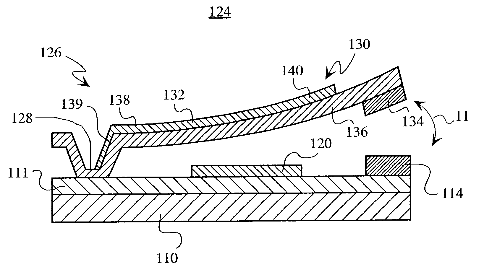
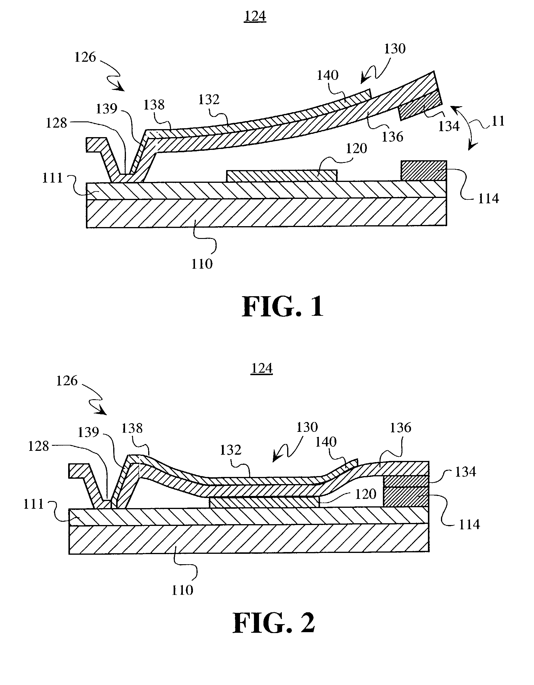
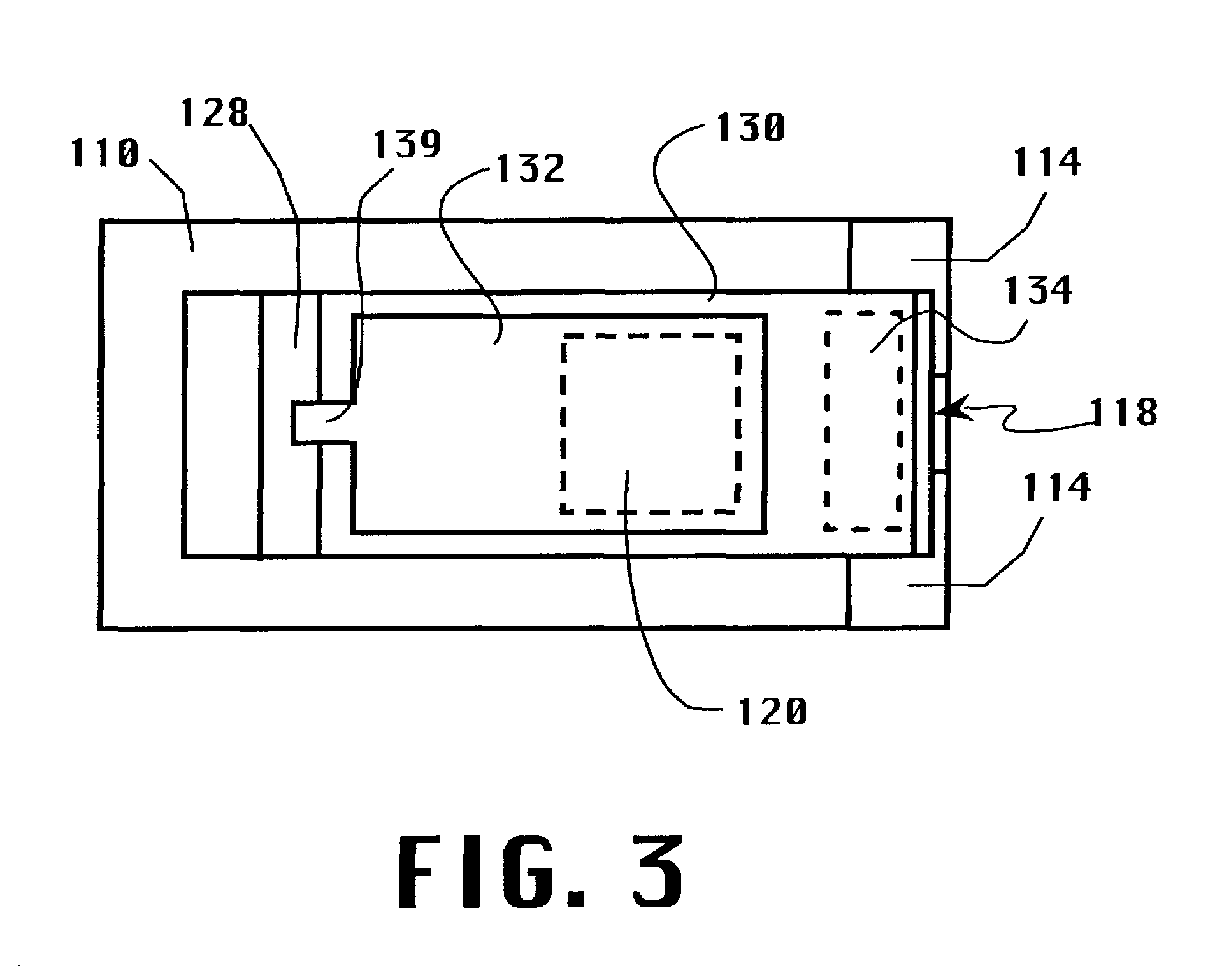
[0038]The present disclosure describes a miniature RF switch designed for applications over a frequency range from DC to approximately 100 GHz. The following disclosure describes an RF MEMS switch according to the present invention fabricated on a silicon-based substrate. However, RF MEMS switches according to the present invention may also be fabricated from various other substrate materials, such as gallium arsenide (GaAs), glass, and other dielectrics.

[0039]In a preferred embodiment, a micro-electromechanical switch, generally designated 124 and best illustrated in FIGS. 1, 2 and 3, is fabricated on a substrate 110 using generally known microfabrication techniques, such as masking, etching, deposition, and lift-off. In a preferred embodiment, the RF MEMS switch 124 is directly formed on the substrate 110 and monolithically integrated with a transmission line 114. Alternatively, the RF MEMS switch 124 may be discreetly formed and then bonded to the substrate 110. The switch 124 co...


PUM


Abstract

A micro-electromechanical system (MEMS) switch formed on a substrate, the switch comprising a transmission line formed on the substrate, a substrate electrostatic plate formed on the substrate, and an actuating portion. The actuating portion comprises a cantilever anchor formed on the substrate and a cantilevered actuator arm extending from the cantilever anchor. Attraction of the actuator arm toward the substrate brings an electrical contact into engagement with the portions of the transmission line separated by a gap, thus bridging the transmission line gap and closing the circuit. In order to maximize electrical isolation between the transmission line and the electrical contact in an OFF-state while maintaining a low actuation voltage, the actuator arm is bent such that the minimum separation distance between the transmission line and the electrical contact is equal to or greater than the maximum separation distance between the substrate electrostatic plate and arm electrostatic plate.

Description

[0001]This application claims priority under 35 U.S.C. 119(e) to co-pending U.S. Patent Application No. 60 / 324,244 (filed on 21 Sep. 2001) entitled “STRESS BIMORPH RF MEMS SWITCHES,” the contents of which are hereby expressly incorporated herein in their entirety by this reference.BACKGROUND[0002]1. Field[0003]The present invention relates to micro-electromechanical systems (MEMS) and, in particular, to a micromachined electromechanical radio frequency (RF) switch that can preferably function over a range of signal frequencies from 0 Hz to approximately 100 GHz.[0004]2. Description of Related Art[0005]MEMS (micro-electromechanical system) switches have a wide variety of uses in both military and commercial applications. For example, electrostatically actuated micro-electromechanical switches can conduct RF current in applications involving the use of antenna phase shifters, in the tuning of reconfigurable antenna elements, and in the fabrication of tunable filters.[0006]A representa...

Claims


Application Information

Patent Timeline
Patent Type & Authority Patents(United States)
IPC IPC(8): H01H51/22H01H1/20H01H59/00
CPCH01H59/0009H01G5/40H01G5/18H01H1/20H01H2059/0018H01H2059/0081H01H2059/0072
Inventor SCHWARTZ, ROBERT N.WU, MINGHSU, TSUNG-YUANSCHMITZ, ADELE E.LOO, ROBERT Y.SCHAFFNER, JAMES H.TANGONAN, GREGORY L.
Owner HRL LAB
Why Eureka
Try Eureka