Cleaving process to fabricate multilayered substrates using low implantation doses

a technology of implantation dose and fabrication process, which is applied in the field of manufacturing objects, can solve the problems of difficult high implantation cost, and difficulty in efficient production of simox wafers, and achieve the effect of improving film quality and efficiency

Inactive Publication Date: 2006-06-06
SILICON GENERAL CORPORATION
View PDF257 Cites 127 Cited by
  • Summary
  • Abstract
  • Description
  • Claims
  • Application Information

AI Technical Summary

Benefits of technology

[0011]According to the present invention, a technique including a method and device for manufacturing objects is provided. In an exemplary embodiment, the present invention provides a method for fabricating multilayered substrates from a cleaving process. Such substrates use low doses of particles, which are used to create stress in a cleaving layer. The low doses of particles improve film quality and efficiency of the present method.
[0016]Numerous benefits are achieved over pre-existing techniques using the present invention. In particular, the present invention uses controlled energy and selected conditions to preferentially cleave a thin film of material from a donor substrate which includes multi-material sandwiched films. This cleaving process selectively removes the thin film of material from the substrate while preventing a possibility of damage to the film or a remaining portion of the substrate. In other aspects, the process also provides a multilayered substrate structure, which can be reused without substantial damage. Accordingly, the remaining substrate portion can be re-used repeatedly for other applications. Still further, the method provides smoother films (e.g., less than 30 or 20 or 10 or 5 or 3 or 2 Angstroms RMS) upon cleaving. Depending upon the application, one or more of these advantages may exist.

Problems solved by technology

SIMOX wafers, however, have numerous limitations.
For example, SIMOX wafers are often difficult to make in an efficient manner, since the high doses often require a long implantation time.
Implantation is generally an expensive operation in the manufacture of wafers.
Additionally, implantation of oxygen often causes damage to the device layer.
Such damage can influence the operation and reliability of integrated circuit devices that are fabricated onto the device layer.
This thermal blistering technique for manufacturing SOI wafers has many limitations.
For high volume production, the high doses of hydrogen often requires the use of many ion implanters, which are expensive and difficult to maintain.
Additionally, thermal blistering often creates rough surface finishes, which can produce worthless scrap product.
Such thermal treatment process would often require a high temperature, which would lead to an exceedingly rough and imprecise fracture morphology along the microcavity plane.
Accordingly, the Bruel '970 also requires high temperatures, which are generally undesirable and lead to excessive surface roughness characteristics.
Unfortunately, this technique is often complicated and expensive.
Moreover, epitaxial growth on a porous layer can compromise the quality of the epitaxial film by the introduction of defects into it, which is very undesirable.
Other limitations can also exist with such technique.

Method used


Image

  • Cleaving process to fabricate multilayered substrates using low implantation doses
  • Cleaving process to fabricate multilayered substrates using low implantation doses
  • Cleaving process to fabricate multilayered substrates using low implantation doses

Examples


example

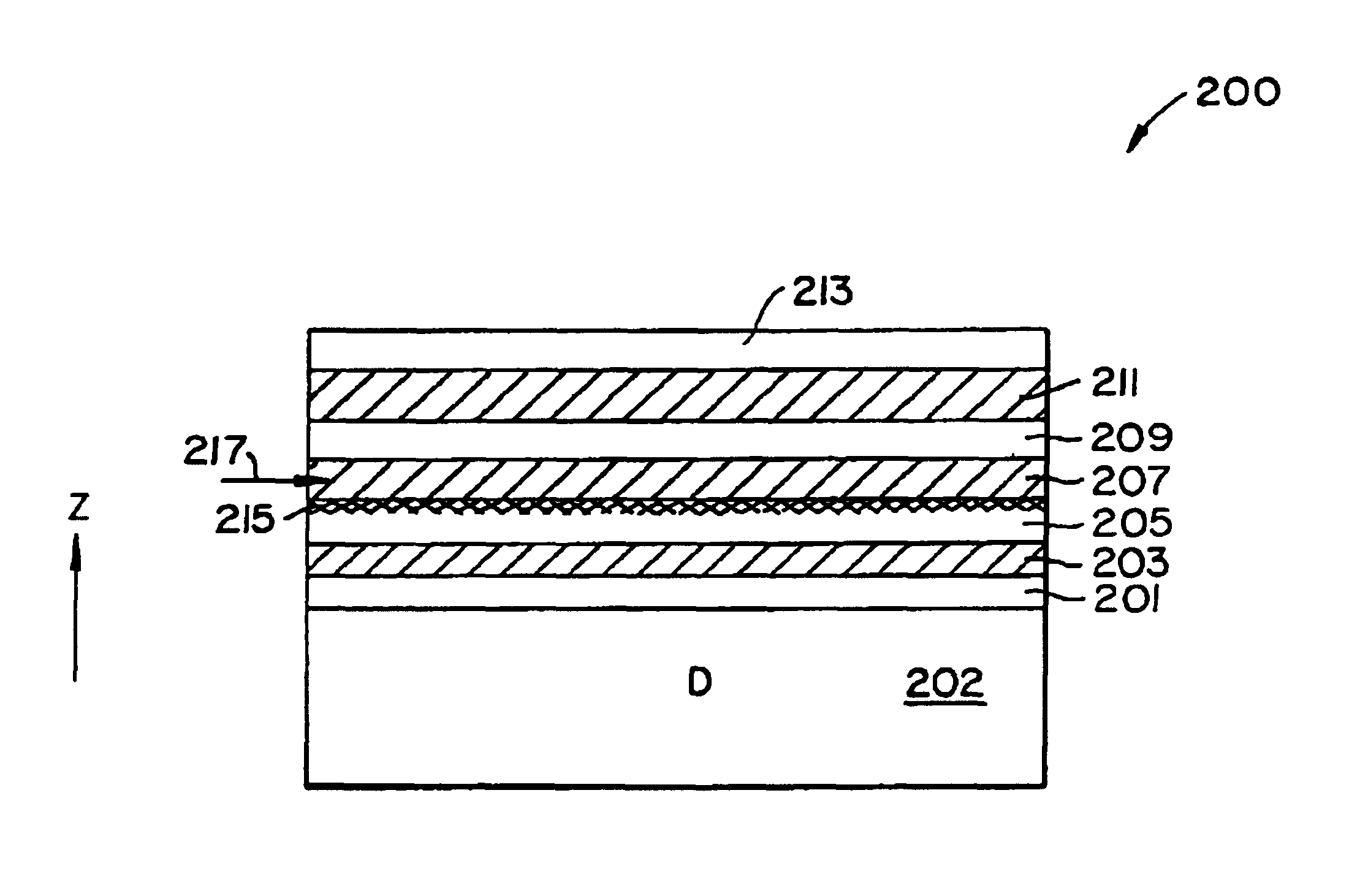
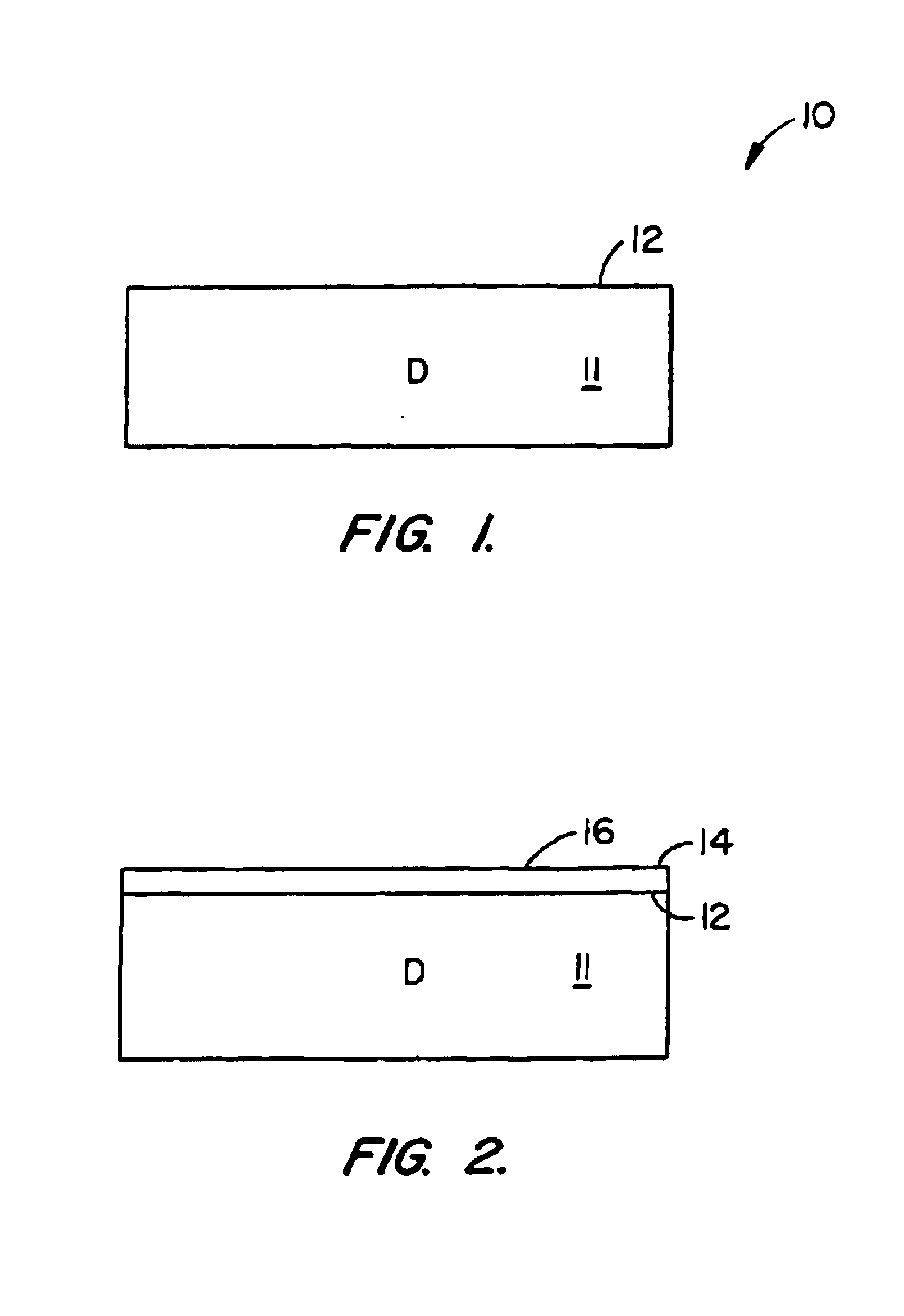
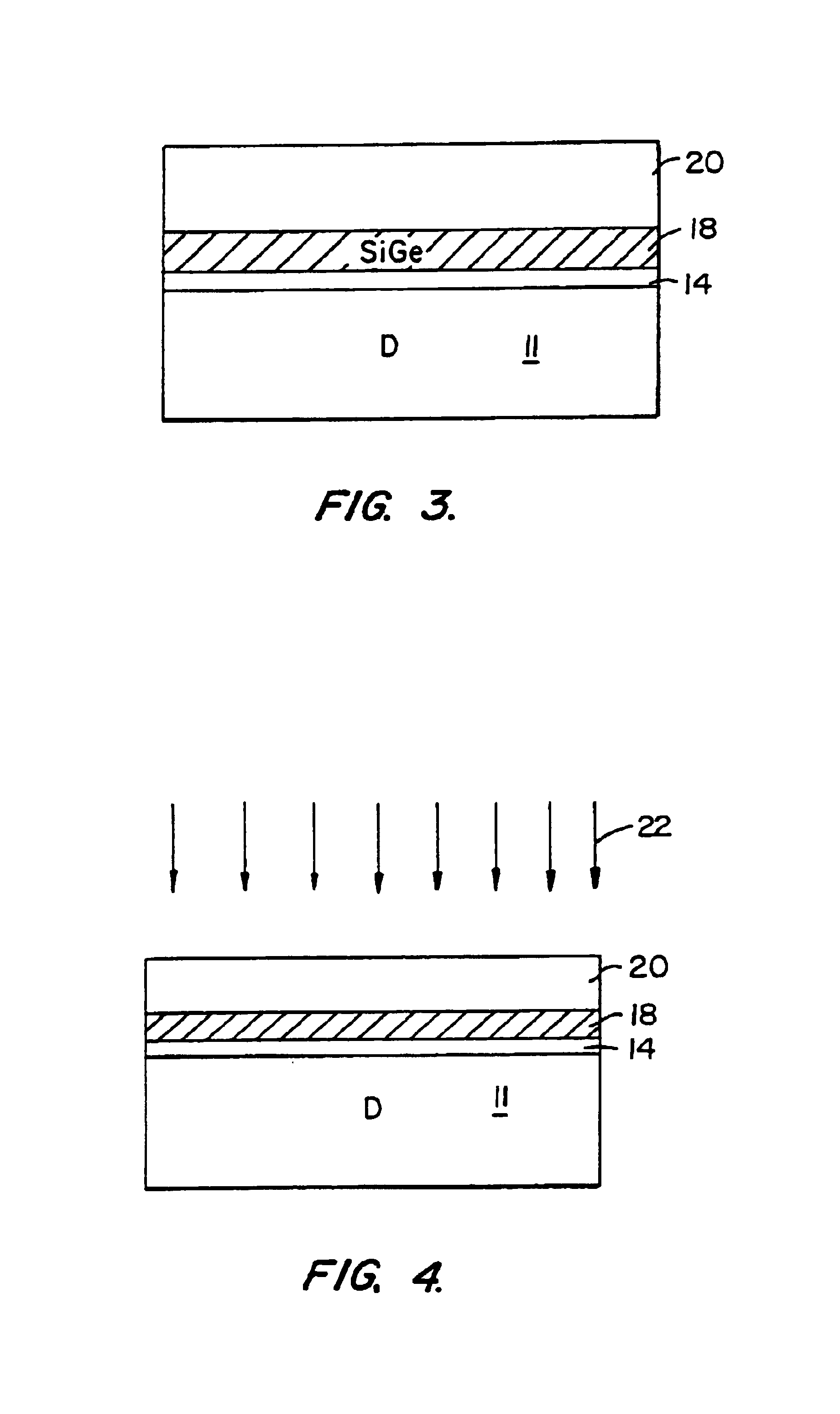
[0052]To prove the principle and operation of the present invention, an experiment was performed. In this experiment, we used eight-inch bulk CZ wafers. These wafers were prime low boron concentration wafers from Mitsubishi Silicon America. The wafers were cleaned using a conventional SC1 and SC2 clean. Next, the wafers were dried using a conventional spin rinse dry so that the wafers were free from liquid droplets. Each wafer was loaded into an epitaxial silicon reactor. The reactor was a tool made by ASM International of Phoenix, Arizona, but is not limited to such reactor. A high temperature bake at about 1,100 Celsius was performed on the wafer. This bake removed native oxide and cleaned faces of the wafer. The bake was followed by a deposition process, where about 2,000 Angstroms of epitaxial silicon was deposited.

[0053]Such deposition was provided by a combination of silane and hydrogen gases in a conventional manner.

[0054]Next, the method used a deposition of silicon germaniu...


PUM


Abstract

A method of forming substrates, e.g., silicon on insulator, silicon on silicon. The method includes providing a donor substrate, e.g., silicon wafer. The method also includes forming a cleave layer on the donor substrate that contains the cleave plane, the plane of eventual separation. In a specific embodiment, the cleave layer comprising silicon germanium. The method also includes forming a device layer (e.g., epitaxial silicon) on the cleave layer. The method also includes introducing particles into the cleave layer to add stress in the cleave layer. The particles within the cleave layer are then redistributed to form a high concentration region of the particles in the vicinity of the cleave plane, where the redistribution of the particles is carried out in a manner substantially free from microbubble or microcavity formation of the particles in the cleave plane. That is, the particles are generally at a low dose, which is defined herein as a lack of microbubble or microcavity formation in the cleave plane. The method also includes providing selected energy to the donor substrate to cleave the device layer from the cleave layer at the cleave plane, whereupon the selected energy is applied to create a controlled cleaving action to remove the device layer from a portion of the cleave layer in a controlled manner.

Description

[0001]This is a continuation of Ser. No. 09 / 370,959 filed Aug. 10, 1999, abnd.BACKGROUND OF THE INVENTION[0002]The present invention relates to the manufacture of objects. More particularly, the invention provides a technique including a method and device for cleaving a substrate in the fabrication of a multi-layered substrate for semiconductor integrated circuits, for example. But it will be recognized that the invention has a wider range of applicability; it can also be applied to other substrates for multi-layered integrated circuit devices, three-dimensional packaging of integrated semiconductor devices, photonic devices, piezoelectronic devices, microelectromechanical systems (“MEMS”), sensors, actuators, solar cells, flat panel displays (e.g., LCD, AMLCD), biological and biomedical devices, and the like.[0003]Many ways of fabricating substrates for the manufacture of integrated circuits have been proposed. In the early days, conventional integrated circuits were fabricated on ...

Claims


Application Information

Patent Timeline
Patent Type & Authority Patents(United States)
IPC IPC(8): H01L21/8238H01L21/46H01L21/76H01L21/02H01L21/265H01L21/301H01L21/762H01L27/12
CPCH01L21/26506H01L21/76254H01L21/76251H01L21/2658
Inventor HENLEY, FRANCOIS J.BRYAN, MICHAEL A.EN, WILLIAM G.
Owner SILICON GENERAL CORPORATION
Why Eureka
Try Eureka