Method and apparatus of growing a thin film

a thin film and film technology, applied in the direction of crystal growth process, chemical vapor deposition coating, coating, etc., can solve the problems of poor heat transfer from the heated surface to the substrate by conduction through the low-pressure gas and by the convection of the low-pressure gas, the reactor presented in u.s. pat. no. 5,879,459 is expensive for batch processing of substrates, etc., to increase the throughput of the ald process, simplify the requirements for reaction space tolerance tolerance tolerance toleran

Inactive Publication Date: 2006-06-13
ASM INTERNATIONAL
View PDF38 Cites 11 Cited by
  • Summary
  • Abstract
  • Description
  • Claims
  • Application Information

AI Technical Summary

Benefits of technology

[0020]Another aspect of the present invention is a method for growing a thin film on a plurality of substrates, which each have a width and a length, in a reaction space according to the ALD method. The method comprises repeatedly and alternately feeding vapor-phase reactants into the reaction space in a form of vapor-phase pulses to form a gas flow in the reaction space, turning the gas flow at least once approximately 180 degrees in the direction of the gas flow; and causing the vapor-phase reactants to react with the surfaces of the substrates to form a thin film compound on the substrates.
[0021]The embodiments summarized above have several advantages. For example, in cases where it takes a long time for depositing a thin film on the wafer, it is advantageous to increase the throughput of the ALD process with batch type processing. In order to increase the robustness of the reactor it is an advantage to simplify the requirements for reaction space tolerances. Source chemicals flow through a long, folded, single reaction space path and the the chemicals cannot choose between competitive parallel flow paths through the reaction space. The deposition processes done in a folded single channel reaction space structure are less sensitive to source chemical pulse and inert gas purge times than the deposition processes done in a parallel reaction space. The folded reaction space is less sensitive to the changes of the local flow channel dimensions when the temperature changes. Mechanical stress may bend metal plates especially when the reaction space is heated for the first time after mechanical cleaning of the reaction chamber parts, e.g., by glass bead blowing. Moreover, it is a benefit that no sealing surfaces are rubbed against each other, and thus the generation of particles is suppressed.
[0022]A multiple heated susceptor-based batch system also has a distinct advantage in reduced heat-up time. In addition susceptors prevent unwanted backside deposition.

Problems solved by technology

There are a number of disadvantages and problems related to the cited known art.
A fundamental problem of conventional batch systems is their dependence on radiative heat transfer due to the poor conduction through the gas at lower pressures typically employed in ALD.
At low pressures, the heat transfer from the heated surfaces to the substrates by conduction through the low-pressure gas and by the convection of the low-pressure gas is poor.
Furthermore, the reactor presented in U.S. Pat. No. 5,879,459 is expensive for batch processing of substrates because of the complex structure and the large number of costly parts.
A problem particularly related to the apparatus of U.S. Pat. No. 6,042,652 is that stringent requirements must be placed on the tightness of the flow distributors to ensure that the distribution of gases is even for each substrate compartment.
In addition, the reactor presented in published PCT patent application WO 00 / 79576 can be used only for processing single substrates and the design with a plasma electrode is not meant for batch processing.

Method used


Image

  • Method and apparatus of growing a thin film
  • Method and apparatus of growing a thin film
  • Method and apparatus of growing a thin film

Examples


Embodiment Construction

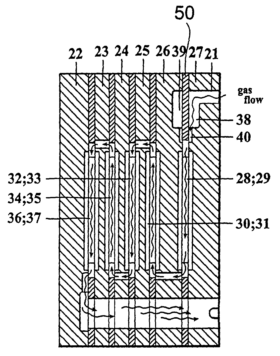
[0043]One embodiment of the present invention involves a method of growing a thin film onto a substrate, in which method a plurality of substrates are placed in serial alignment in a reaction chamber formed by an elongated reaction channel and each actual substrate is subjected to surface reactions of a plurality of vapor-phase reactants according to the ALD method to form a thin film.

[0044]A typical pulsing sequence used for ALD growth of thin film consists of four basic steps:[0045]1. first source chemical pulse[0046]2. first purging period[0047]3. second source chemical pulse[0048]4. second purging period

[0049]These four steps are repeated until a thin film of predetermined thickness is obtained. The purging periods may comprise of inert gas purging optionally combined with or replaced with a vacuum pump down of the reaction space. An advanced pulsing sequence may comprise, e.g., three different source chemical pulses that are separated from each other with reactor removal period...


PUM

PropertyMeasurementUnit
angleaaaaaaaaaa
angleaaaaaaaaaa
angleaaaaaaaaaa

Abstract

A method and apparatus for growing a thin film onto a substrate is disclosed. According to one embodiment, a plurality of substrates, each having a width and a length, are placed in a reaction space and the substrates are subjected to surface reactions of vapor-phase reactants according to the ALD method to form a thin film on the surfaces of the substrates. The reaction space comprises an elongated gas channel having a cross-section with a width greater that the height and which has a length which is at least 2 times greater than the length of one substrate in the direction of the gas flow in the channel, the channel having a folded configuration with at least one approximately 180 degree turn in the direction of the gas flow.

Description

PRIORITY INFORMATION[0001]This application is a continuation-in-part of U.S. patent application Ser. No. 09 / 836,674, filed Apr. 16, 2001, which claims the priority under 35 U.S.C. §119 of Finnish Patent Application No. 20000899, filed Apr. 14, 2000, and this application claims the priority under 35 U.S.C. §119 of Finnish Patent Application No. 20011998, filed Oct. 12, 2001, the disclosures of these applications are hereby incorporated herein by reference in their entirety.BACKGROUND OF THE INVENTION[0002]1. Field of the Invention[0003]The present invention relates to the production of thin films and, in particular, to methods and apparatus for producing a thin film on a substrate by subjecting the substrate to repeated pulses of gas or vapor-phase reactants.[0004]2. Description of the Related Art[0005]Atomic Layer Deposition (abbreviated “ALD”), which was formerly called Atomic Layer Epitaxy or “ALE,” is a method in which thin films are grown on the surface of a substrate by subject...

Claims


Application Information

Patent Timeline
Patent Type & Authority Patents(United States)
IPC IPC(8): C30B23/00C23C16/44C23C16/455C23C16/458C30B25/02C30B25/08C30B25/14
CPCC23C16/45502C23C16/45546C30B25/14C30B25/02C30B25/08C23C16/4583
Inventor LINDFORS, SVENRAAIJMAKERS, IVO
Owner ASM INTERNATIONAL
Why Eureka
Try Eureka