
Lithium-drifted silicon detector with segmented contacts

a silicon detector and segmented contact technology, applied in the direction of semiconductor devices, solid-state devices, electrical apparatus, etc., can solve the problems of increasing the size and complexity of the detector, affecting the fabrication efficiency of the detector, and the difficulty of electrical connection to the substrate, etc., to achieve the effect of convenient fabrication

Inactive Publication Date: 2006-06-13
RGT UNIV OF CALIFORNIA
View PDF3 Cites 9 Cited by
  • Summary
  • Abstract
  • Description
  • Claims
  • Application Information

AI Technical Summary

Benefits of technology

[0016]It is the general objective of this invention to provide radiation detectors which are readily fabricated and which may be utilized at room temperatures. Taught within the present invention are several detector embodiments including those fabricated from Si (i.e. (Si(Li)), Ge, and CdZnTe.
[0032]Another aspect of the invention is the creation of radiation detectors that exhibit low leakage current thereby increasing the achievable signal-to-noise ratio.

Problems solved by technology

Ge detectors continue to increase in size and complexity.
Although this is a viable process, it suffers from device pitch limitations (number of segments per mm).
In the case of the gold surface barrier (p-type), the adhesion of the gold to the silicon surface is also very poor, making electrical connection to the substrate difficult and rendering the contact prone to failure.

Method used


Image

  • Lithium-drifted silicon detector with segmented contacts
  • Lithium-drifted silicon detector with segmented contacts
  • Lithium-drifted silicon detector with segmented contacts

Examples


Embodiment Construction

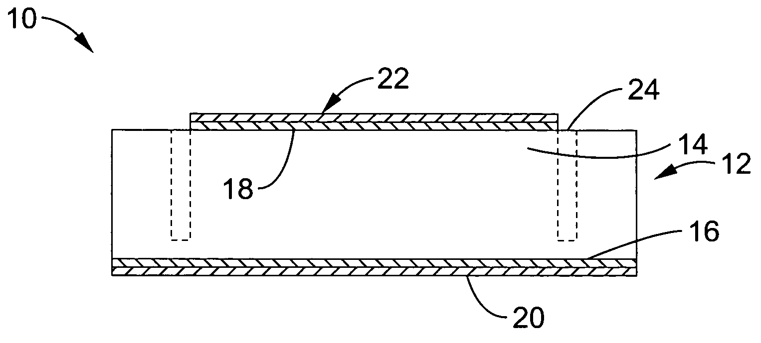
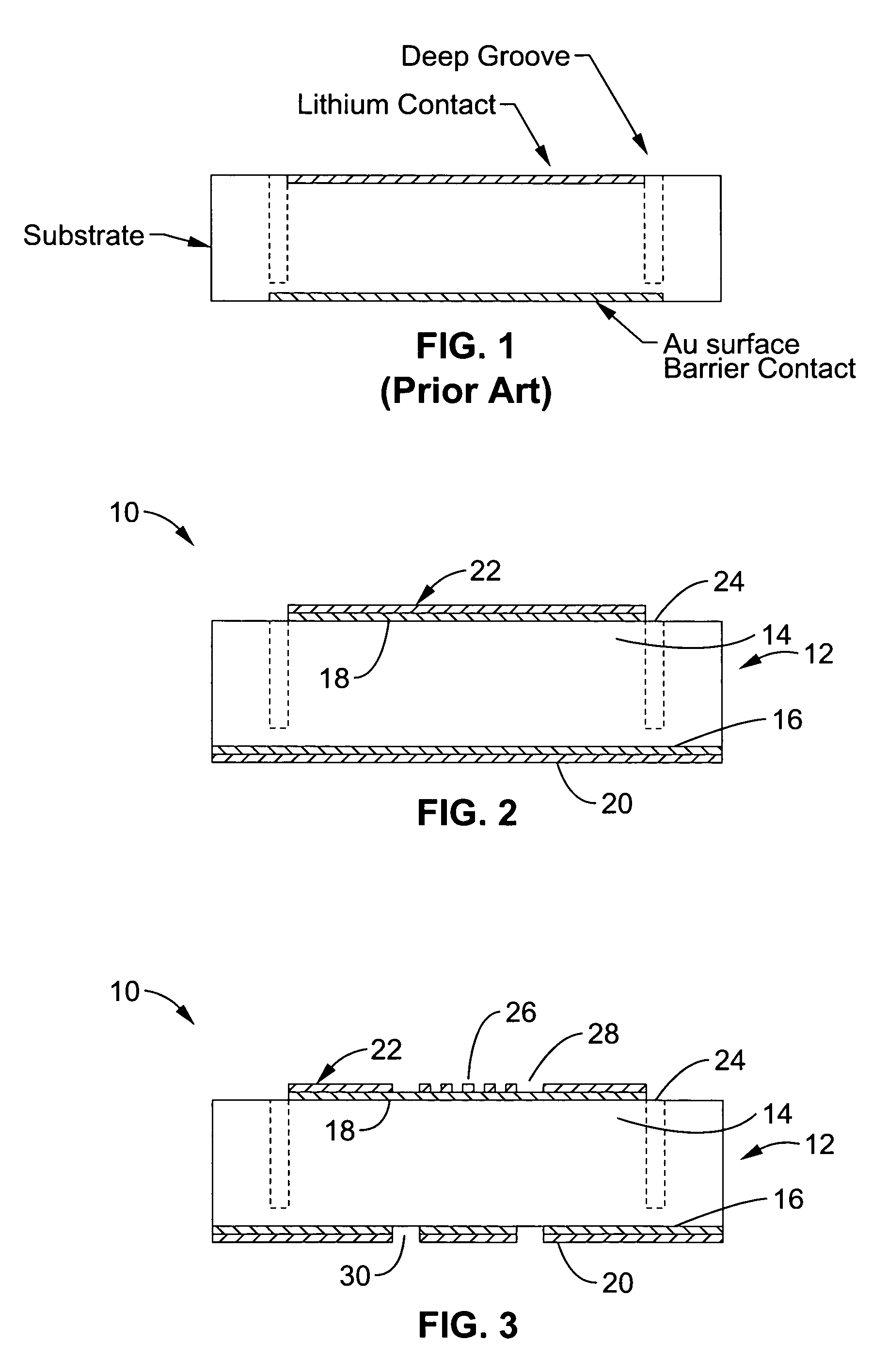
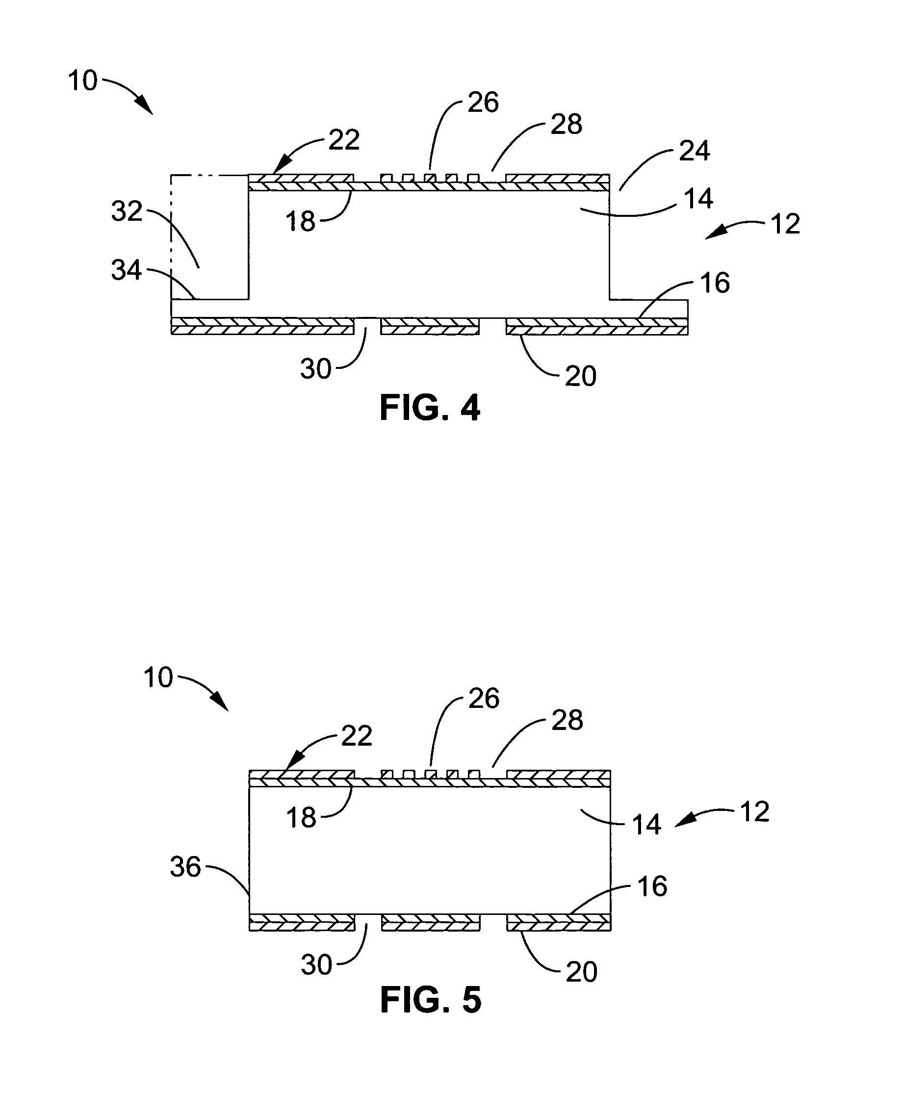
[0047]Referring more specifically to the drawings, for illustrative purposes the present invention is embodied in the apparatus generally shown in FIG. 2 through FIG. 11B. It will be appreciated that the apparatus may vary as to configuration and as to details of the parts, and that the method may vary as to the specific steps and sequence, without departing from the basic concepts as disclosed herein.

[0048]Embodiments of semiconductor radiation detectors are taught within the present invention. Although other semiconductor materials may be utilized, the invention describes embodiments utilizing silicon, germanium and CdZnTe.

Lithium-Drifted Silicon Compensation

[0049]Lithium-drifted silicon (Si(Li)) is a charge-compensated, or more simply compensated, material with reduced net ionic charge in the bulk crystalline Si material. This aspect is particularly important for use in radiation detectors having thicknesses ranging from 1–10 mm or more. Lithium drifting is more accurately stated...


PUM


Abstract

A method and apparatus for creating both segmented and unsegmented radiation detectors which can operate at room temperature. The devices include a metal contact layer, and an n-type blocking contact formed from a thin layer of amorphous semiconductor. In one embodiment the material beneath the n-type contact is n-type material, such as lithium compensated silicon that forms the active region of the device. The active layer has been compensated to a degree at which the device may be fully depleted at low bias voltages. A p-type blocking contact layer, or a p-type donor material can be formed beneath a second metal contact layer to complete the device structure. When the contacts to the device are segmented, the device is capable of position sensitive detection and spectroscopy of ionizing radiation, such as photons, electrons, and ions.

Description

CROSS-REFERENCE TO RELATED APPLICATIONS[0001]This application claims priority from U.S. provisional application Ser. No. 60 / 470,087 filed on May 12, 2003, incorporated herein by reference in its entirety. This application also claims priority from U.S. provisional application Ser. No. 60 / 547,926 filed on Feb. 25, 2004, incorporated herein by reference in its entirety.STATEMENT REGARDING FEDERALLY SPONSORED RESEARCH OR DEVELOPMENT[0002]This invention was made with U.S. Government support under Contract Number DE-AC03-76SF00098 between the U.S. Department of Energy and The Regents of the University of California for the management and operation of the Lawrence Berkeley National Laboratory. The U.S. Government has certain rights in this invention.INCORPORATION-BY-REFERENCE OF MATERIAL SUBMITTED ON A COMPACT DISC[0003]Not ApplicableNOTICE OF MATERIAL SUBJECT TO COPYRIGHT PROTECTION[0004]A portion of the material in this patent document is subject to copyright protection under the copyri...

Claims


Application Information

Patent Timeline
Patent Type & Authority Patents(United States)
IPC IPC(8): H01L21/00H01L31/0288H01L31/0376H01L31/103H01L31/18
CPCH01L31/0288H01L31/1804H01L31/103Y02E10/547
Inventor TINDALL, CRAIG S.LUKE, PAUL N.
Owner RGT UNIV OF CALIFORNIA
Learn More