Ion implantation method, SOI wafer manufacturing method and ion implantation system

Active Publication Date: 2006-06-20
APPLIED MATERIALS INC
View PDF35 Cites 33 Cited by
  • Summary
  • Abstract
  • Description
  • Claims
  • Application Information

AI Technical Summary

Benefits of technology

[0009]The present invention was made to deal with the foregoing problems inherent in the prior art, and objects of the invention are to provide an ion implantation method which can achieve sufficient throughput by increasing a b

Problems solved by technology

With the ion source of this type, it is relatively difficult to generate high-density plasma only by electric arc discharge.
Therefore, in processes of forming a t

Method used


Image

  • Ion implantation method, SOI wafer manufacturing method and ion implantation system
  • Ion implantation method, SOI wafer manufacturing method and ion implantation system
  • Ion implantation method, SOI wafer manufacturing method and ion implantation system

Examples


Embodiment Construction

[0039]The preferred embodiments of the present invention will now be described with reference to the accompanying drawings. In the drawings, similar or equivalent portions will be denoted by similar reference numerals, and repeated explanation will be omitted.

[0040]First, an ion implantation method and an ion implantation system will be described.

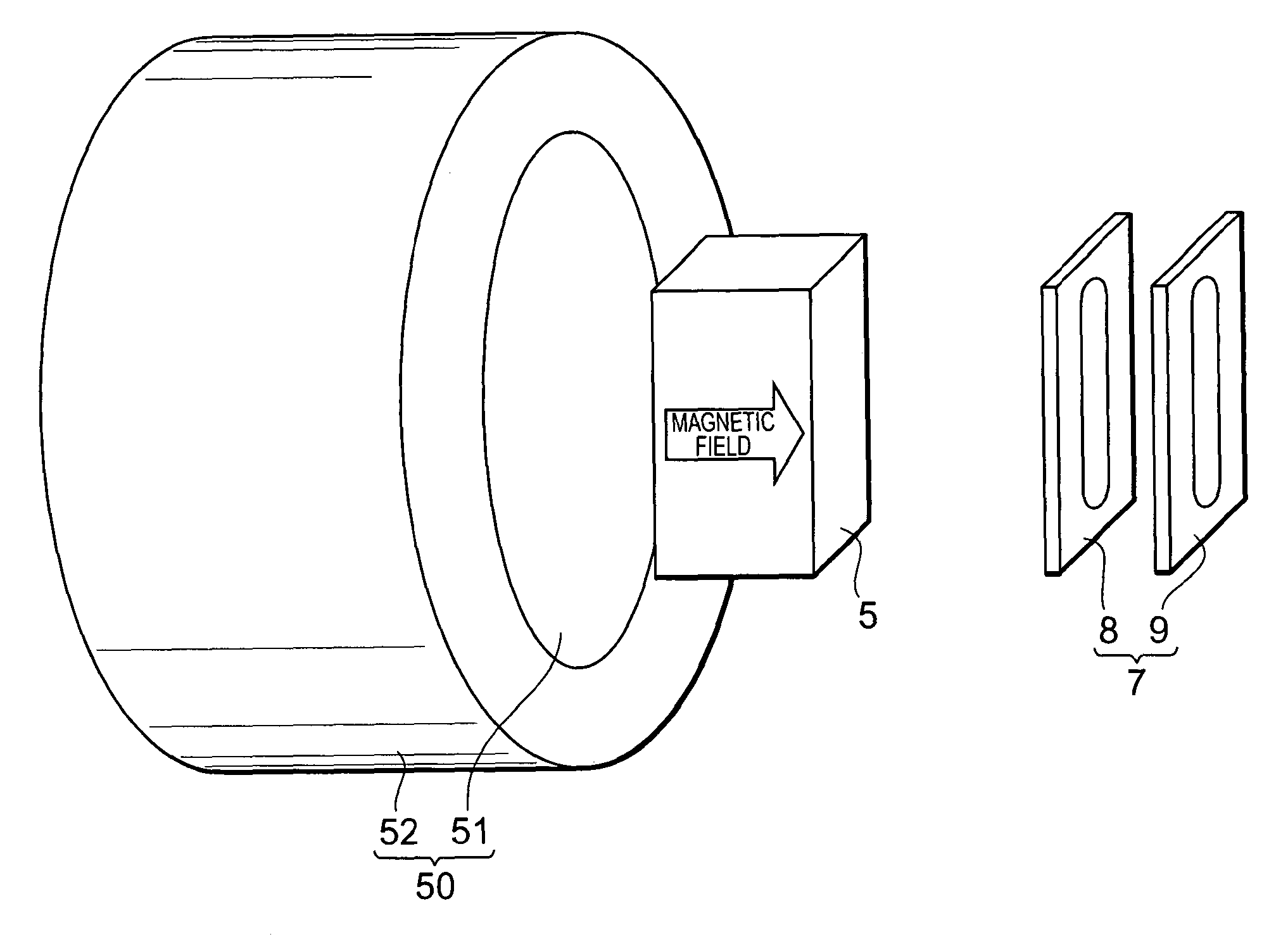
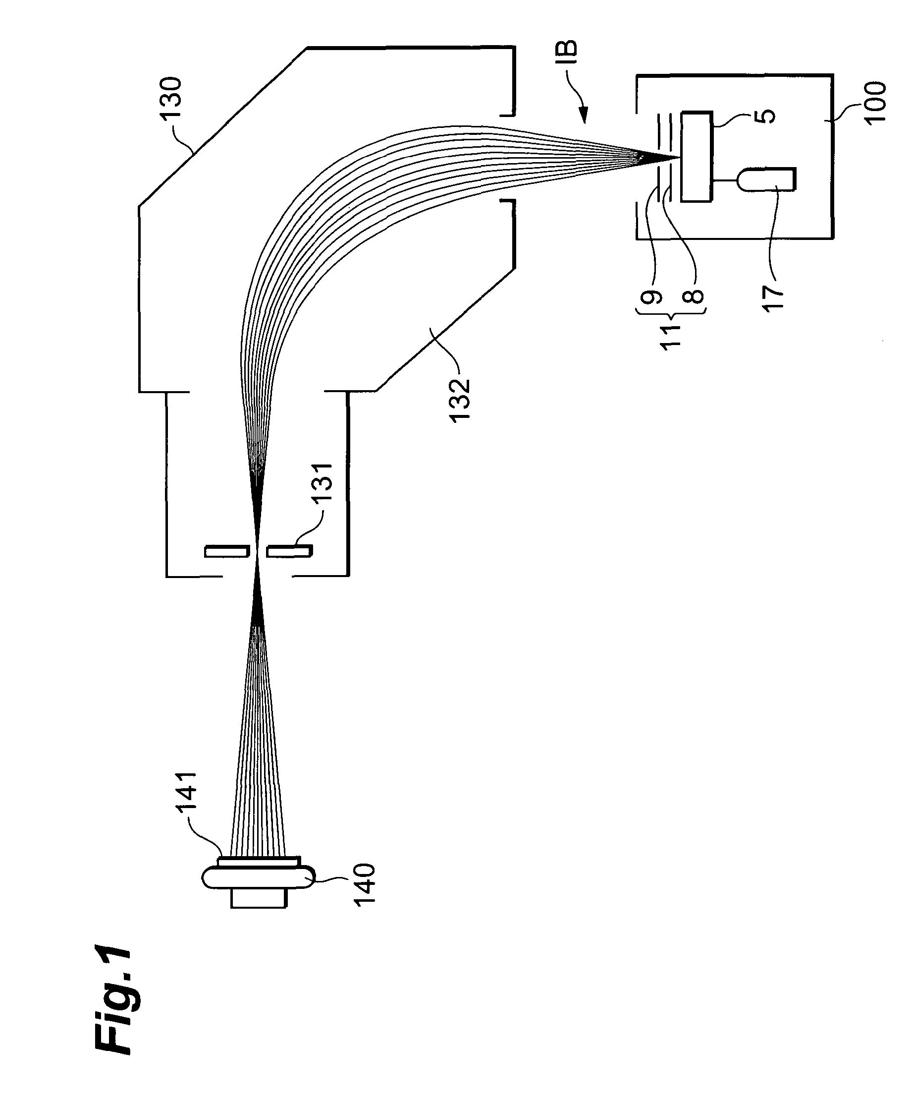
[0041]FIG. 1 is an explanatory view schematically showing an example of an ion implantation system of the present invention. The system shown in FIG. 1 comprises an ion extraction assembly 100 which includes an arc discharge ion source 5, a cylinder 17 for supplying predetermined gas to the ion source 5 and a pair of extraction electrodes 8 and 9; an ion mass selector 130; and a target substrate holder 140.

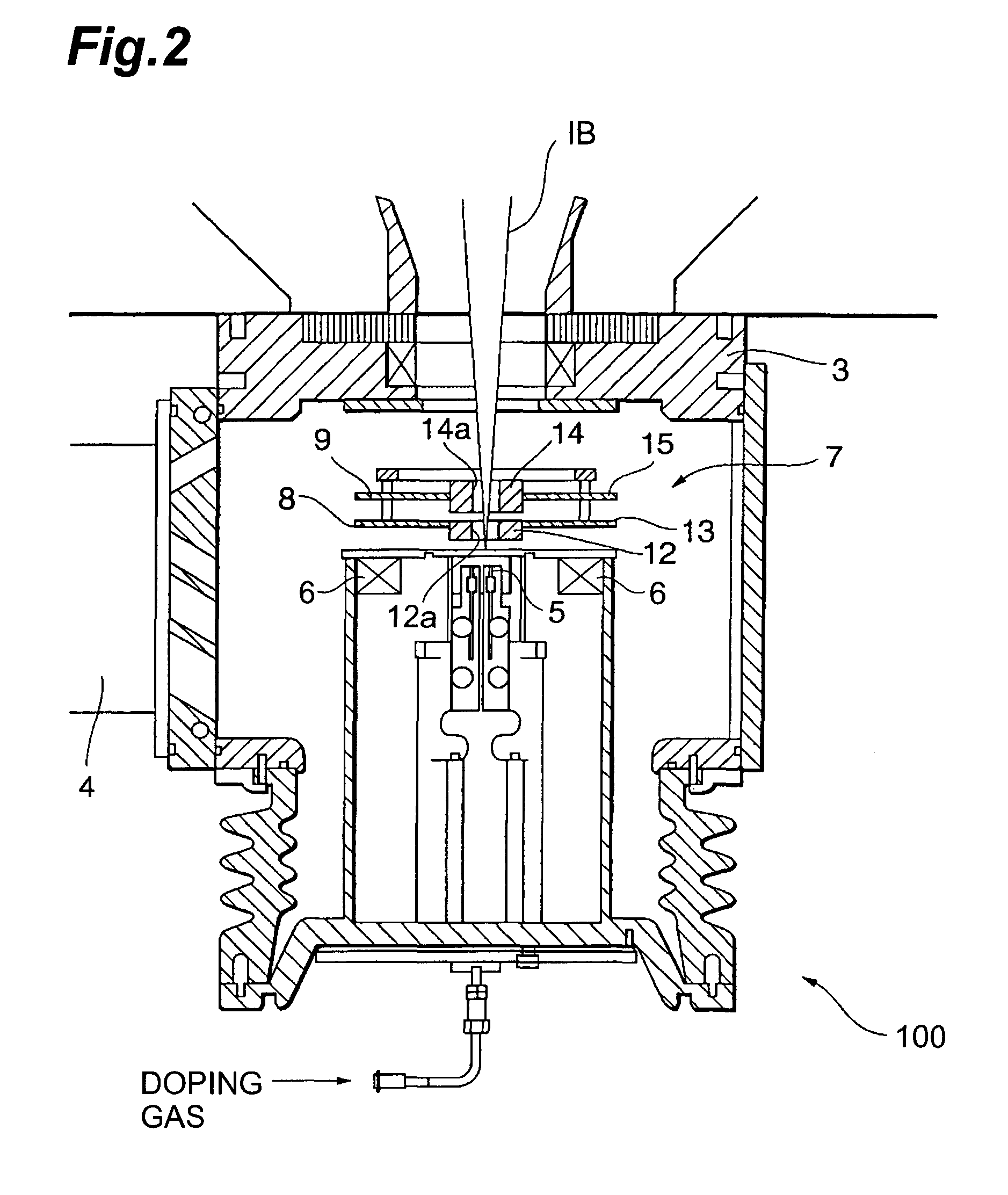
[0042]FIG. 2 is a sectional view showing a schematic constitution of the ion extraction assembly 100. In the drawing, the ion extraction assembly 100 has a source chamber 3, and pressure in this source chamber 3 is reduced to a predetermi...


PUM

PropertyMeasurementUnit
Timeaaaaaaaaaa
Energyaaaaaaaaaa
Ionizing radiationaaaaaaaaaa

Abstract

The present invention provides an ion implantation method which can achieve sufficient throughput by increasing a beam current even in the case of ions with a small mass number or low-energy ions, an SOI wafer manufacturing method, and an ion implantation system. When ions are implanted by irradiating a semiconductor substrate with an ion beam, predetermined gas is excited in a pressure-reduced chamber to generate plasma containing predetermined ions, a magnetic field is formed by a solenoid coil or the like along an extraction direction when the ions are extracted to the outside of the chamber, and the ions are extracted from the chamber with predetermined extraction energy. The formation of the magnetic field promotes ion extraction, but this magnetic field has no influence on an advancing direction of the extracted ions. Therefore, the ion beam current can be kept at a high level-to contribute to the ion implantation.

Description

BACKGROUND OF THE INVENTION[0001]1. Field of the Invention[0002]The present invention relates to an ion implantation method, an SOI wafer manufacturing method and an ion implantation system.[0003]2. Description of the Related Art[0004]In a field of IC devices, a method for implanting predetermined ions in a semiconductor substrate has conventionally been used when a transistor junction is formed.[0005]Ion implantation is also used in a smart cut method which is one of the manufacturing methods of silicon-on-insulator (SOI) wafers (Japanese Patent Laid-Open Publication No. 2000-12285, etc.). According to the smart cut method, an SOI wafer is manufactured by implanting hydrogen ions in a Si substrate through an insulating layer (SiO2 layer or the like) formed on a surface of the Si substrate, bonding this substrate to another Si substrate and then cutting it at a hydrogen ion implanted layer.[0006]The ion implantation is normally carried out by using an ion implantation system. For an...

Claims


Application Information

Patent Timeline
IPC IPC(8): H01L21/26C23C14/48H01J27/02H01J27/08H01J27/16H01J37/08H01J37/317H01L21/265H01L21/762
CPCH01J37/08H01L21/76254H01L21/26506H01J2237/0817H01J2237/31701H01L21/2658
Inventor ITO, HIROYUKIMATSUNAGA, YASUHIKO
Owner APPLIED MATERIALS INC
Why Eureka
Try Eureka