[0017]An object of the present invention is to provide a
semiconductor device that has an excellent driving capability and a good quality for high-speed operation, with ESD-proof as well as latch-up-proof amply provided, while the element size of an input / output protection circuit section thereof successfully reduced.
[0023]Because the input / output protection circuit section contained in a
semiconductor device of the present invention has, under the first
diffusion layer, a first conductive type well with a lower
dopant concentration than the first
diffusion layer, the base potential of a lateral
parasitic bipolar transistor that is composed of a first and second
diffusion layers and a region sandwiched between these
layers can be readily raised, and the snap-back, easily induced thereto. This enables the present protection circuit to take a lower value of the trigger
voltage Vt1 than the conventional ones. In consequence, the amount of the injection current necessary to make the
parasitic bipolar transistor operate can be reduced, which leads to a higher speed of response. Furthermore, as the condition Vt1<Vt2 can be established, a plurality of transistors composing the protection circuit section all operate alike so that it can be prevented that the surge flows down only to some specific transistors. Therefore, improvements on the ESD-proof as well as on the reliability of the protection circuit section can be attained.
[0025]In the
semiconductor device described above, it is preferable to have a structure, in which the gate
electrode and the
dopant diffusion region of second conductive type are placed over the second conductive type well that is formed on the surface of the semiconductor substrate; and the bottom of the first conductive type well is formed at the same depth as the bottom of the second conductive type well or at a level deeper than the bottom of the second conductive type well. In other words, it is preferable that the gate
electrode of the
field effect transistor and the dopant diffusion region of second conductive type are formed over the second conductive type well, and the first conductive type well has a depth not less than the depth of the second conductive type well. With such a structure, after the breakdown of the drain section, a current flows through the semiconductor substrate that has a higher resistance than the second conductive well, which facilitates the potential of the base region of the afore-mentioned lateral parasitic bipolar transistor to rise and, therefore, makes the trigger voltage Vt1 lowered more effectively. This further improves the quality of the response of the protection circuit section as well as the ESD-proof.
[0031]Because the input / output protection circuit section of this
semiconductor device comprises a complementary
field effect transistor, a surge can flow down through a plurality of lines efficiently so that the quality of high-speed operation of the protection circuit as well as the ESD-proof can be further improved. For the purpose of improving the reliability of the protection circuit, it is preferable that a plurality of N-channel type field effect transistors are provided to compose a complementary
field effect transistor.
[0032]In this semiconductor device, it is preferable to have a structure, in which the gate
electrode of the first
field effect transistor and the first dopant diffusion region are placed over the second conductive type well that is formed on the surface of the semiconductor substrate; and the bottom of the first conductive type well is formed at the same depth as the bottom of the second conductive type well or at a level deeper than the bottom of the second conductive type well. In other words, it is preferable that the gate electrode of the first field effect transistor and the first dopant diffusion region are formed over the second conductive type well, and the first conductive type well has a depth not less than the depth of the second conductive type well. With such a structure, after the breakdown of the drain section, a current flows through the semiconductor substrate that has a higher resistance than the second conductive well, which facilitates the potential of the base region of the afore-mentioned lateral parasitic bipolar transistor to rise and, therefore, makes the trigger voltage Vt1 lowered more effectively. This further improves the quality of the response of the protection circuit section as well as the ESD-proof.
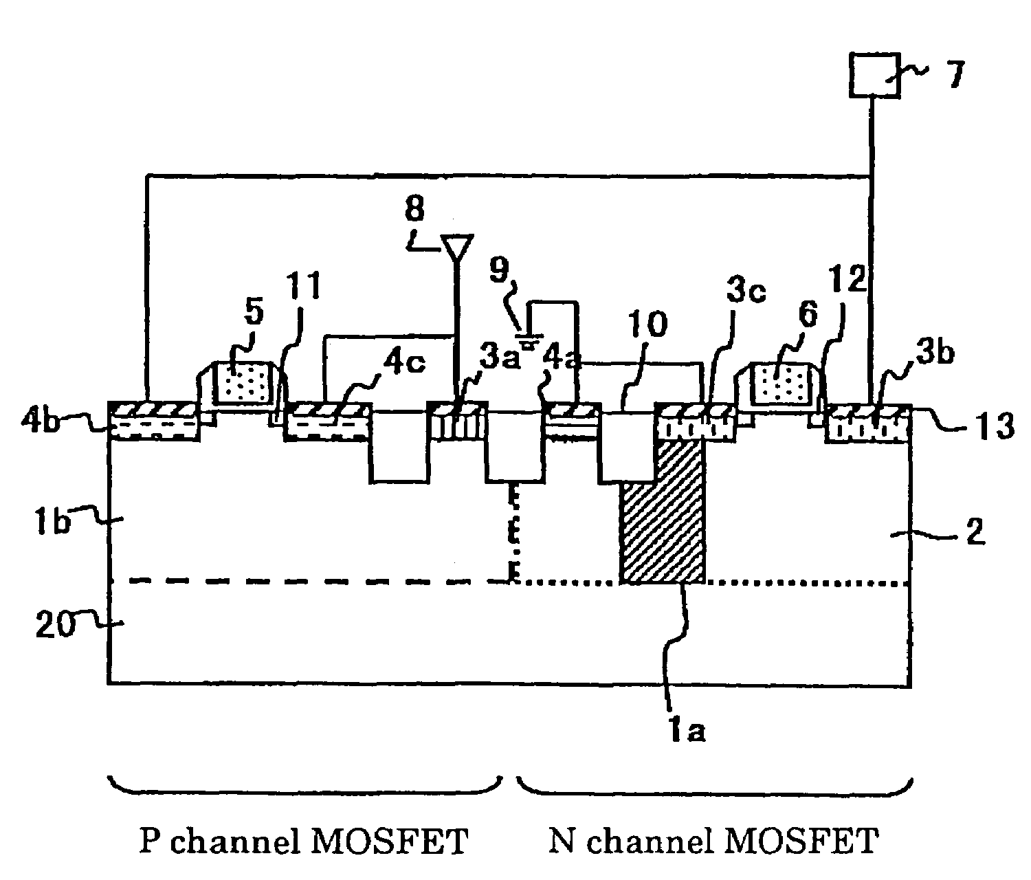
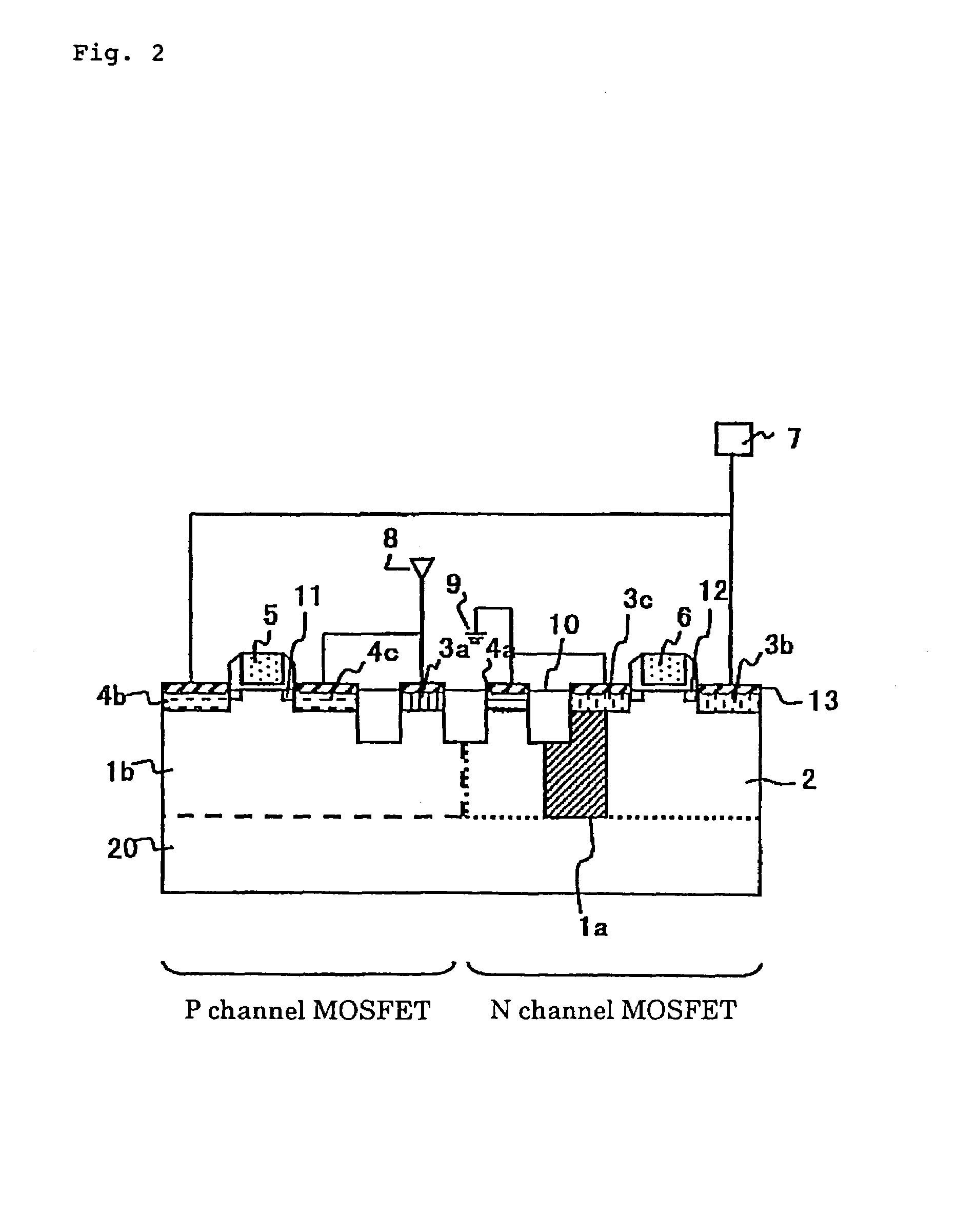
[0033]Further, if this semiconductor device has, in addition, a structure in which, beneath the second conductive type well, there is set a dopant high-concentration region containing second conductive type dopants with a higher dopant concentration than the second conductive type well; and the bottom of the first conductive type well is formed at the same depth as the bottom of the dopant high-concentration region or at a level deeper than the bottom of the dopant high-concentration region, a protection circuit section having a good ESD-proof, together with a good latch-up-proof, can be obtained. As described above, it is well known that setting a dopant high-concentration region at the bottom of the wells can reduce the shunt resistance and improve the latch-up-proof. However, with reducing the shunt resistance, the current
amplification factor of the parasitic bipolar transistor decreases, which makes the parasitic bipolar operations difficult to induce and gives rise to a problem of lowering the ESD-proof. The present invention, hereat, overcomes the above problem by setting a first conductive type well that reaches a depth equal to or deeper than that of the bottom of the dopant high-concentration region. FIG. 3 shows an example with the structure described above, and an N-type well 1a reaching the same depth as the dopant high-concentration region 16 is set therein. With such an N-type well 1a being set, after the breakdown of the drain region 3b, a current starts flowing down through the semiconductor substrate 20 that has a high electric resistance. This facilitates the
electric potential of the base region 2 of the lateral parasitic bipolar transistor to increase and, at the same time, can reduce the trigger voltage Vt1 so that the ESD-proof may be improved. Meanwhile, in the internal circuit region (not shown in the drawing), because the shunt resistance is made smaller by the dopant high-concentration regions 15 and 16, the proof can be a good deal improved against latch-up that may occur between the input / output protection circuit section and the internal circuit region.

