Single electron transistor manufacturing method by electro-migration of metallic nanoclusters

a manufacturing method and technology of nanoclusters, applied in the direction of nanotechnology, electrical equipment, individual molecule manipulation, etc., can solve the problems of high sensitivity of transport properties, difficult nanofabrication technology, and inability to detect tunneling

Active Publication Date: 2006-06-27
STMICROELECTRONICS SRL
View PDF10 Cites 45 Cited by
  • Summary
  • Abstract
  • Description
  • Claims
  • Application Information

AI Technical Summary

Problems solved by technology

Their use involves not only extremely difficult nanofabrication technology (especially challenging for large scale integration), but also some major physics problems including the high sensitivity of transport properties to small variations of the quantum dot size and shape.
An external electric field may be applied to the island using another electrode (“gate”) separated from the island by a thicker insulator, which does not allow noticeable tunneling.
This is of course simply a consequence of the enormous strength of the unscreened Coulomb interaction occurring at low temperatures and, in fact, is the main limitation for the physical implementation of such a kind of single electron devices that are fabricated by scaling down the feature sizes from conventional microelectronics technologies.
However, lithographic and materials limitations restrict the minimum size and composition of such dots (100 nm), and studies are typically limited to sub-Kelvin temperatures.

Method used


Image

  • Single electron transistor manufacturing method by electro-migration of metallic nanoclusters
  • Single electron transistor manufacturing method by electro-migration of metallic nanoclusters
  • Single electron transistor manufacturing method by electro-migration of metallic nanoclusters

Examples


first example

1. Realization of a Patterned Substrate

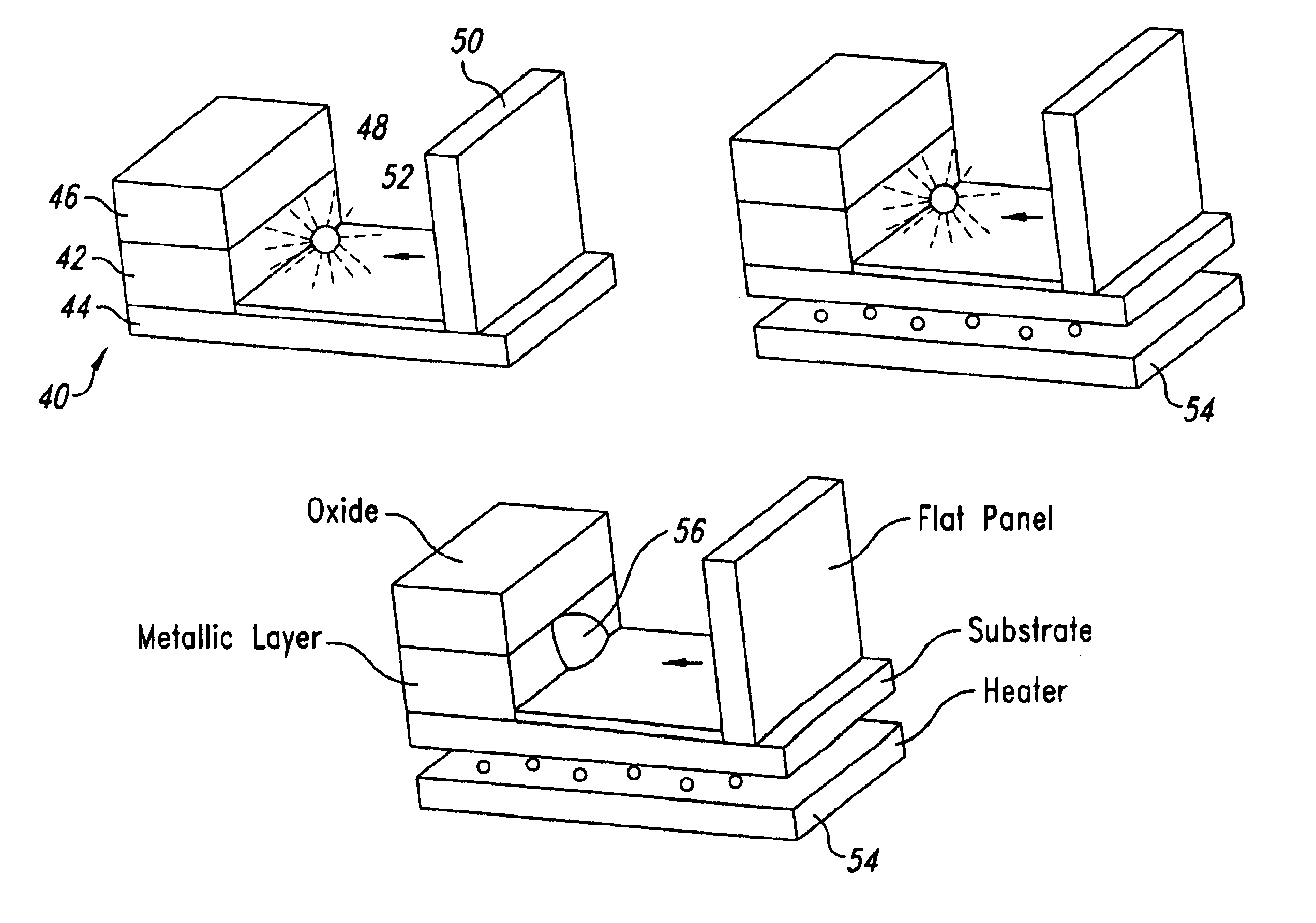
[0069]On a semiconductor substrate 10, for instance a silicon substrate with a silicon oxide layer 12 formed thereon, a rectangular central aperture 14, paths 16 for metallic contacts, and peripheral apertures 18 are opened, leaving a thickness of the oxide layer 12 over the Si substrate 10.

[0070]More particularly, the depth of the aperture can be about three times its width. A high conductive metallic layer 20, for instance a gold layer, is deposited on the contact paths 16 and in the peripheral apertures 18 to form contact pads 22 without invading the central aperture 14.

[0071]Then an oxide layer 24 is deposited on the contact links between the central aperture 14 and the pads 22. Thus, the pads 24 are free-contact surfaces, four in this example, that are available as electrodes for the dielectrophoresis control.

[0072]The described patterned process steps are schematically shown in FIGS. 5A, 5B, 5C.

Deposition of Nanoclusters by Dielectrophore...


PUM


Abstract

A method manufactures a single electron transistor device by electro-migration of nanocluster wherein said nanoclusters are metallically passivated and forced to assembly over a lithographic patterned substrate under control of a non homogeneous electric field at room temperature. A controlled migration and the desired location of the metallic passivated nanoclusters are based on a dielectrophoretic process.

Description

BACKGROUND OF THE INVENTION[0001]1. Field of the Invention[0002]The present invention relates to a manufacturing method for obtaining a single electron transistor by electro-migration of nanocluster.[0003]More specifically, the invention relates to a method for manufacturing a single electron transistor by electro-migration of nanocluster[0004]2. Description of the Related Art[0005]To fully understand all the aspects of the present invention reference is made to the enclosed FIGS. 1-4 showing known examples of single-electron devices.[0006]The enclosed FIG. 1 illustrates the basic concept of single-electronics.[0007]Let's first consider a small electroneutral conductor, traditionally called an island, having exactly as many (m) electrons as protons in its crystal lattice.[0008]In this electroneutral state the island does not generate any appreciable electric field beyond its borders, and a even weak external force {right arrow over (F)} may bring in an additional electron from outsi...

Claims


Application Information

Patent Timeline
Patent Type & Authority Patents(United States)
IPC IPC(8): H01L21/00B82B1/00B82B3/00H01L21/335H01L29/76H01L49/00
CPCB82B3/00B82Y10/00B82Y30/00H01L29/66439H01L49/006B82Y40/00Y10S438/969H10N99/05
Inventor MASCOLO, DANILOSCALDAFERRI, ROSSANANAPOLITANO, TERESACASUSCELLI, VALERIAOCCHIPINTI, LUIGI
Owner STMICROELECTRONICS SRL
Why Eureka
Try Eureka