
Method of simulating patterns, computer program therefor, medium storing the computer program and pattern-simulating apparatus

Active Publication Date: 2006-07-04
JAPAN DISPLAY CENT INC
View PDF7 Cites 6 Cited by
  • Summary
  • Abstract
  • Description
  • Claims
  • Application Information

AI Technical Summary

Benefits of technology

[0010]Accordingly, the present invention is for solving the problem set forth above and provides a method of simulating patterns in which design mista

Problems solved by technology

When exposure data are, however, mistakenly entered into the CAD system for the divided exposure process, although such mistake may be found at an error processing step, it may not be detected until a pattern inspection step performed after patterns are exposed and formed on the substrate.
Further, when the division of reticles is made in error and boundaries between neighboring reticles are not consistent with each other, patterns formed on the substrate short-circuit or are broken so that the substrate is poor in quality.
Particularly, when division lines are made zigzag in shape and are provided with buffer regions in order to make the lines hardly seen, it is not easy to find out patterns mistakenly formed on the substrate.

Method used


Image

  • Method of simulating patterns, computer program therefor, medium storing the computer program and pattern-simulating apparatus
  • Method of simulating patterns, computer program therefor, medium storing the computer program and pattern-simulating apparatus
  • Method of simulating patterns, computer program therefor, medium storing the computer program and pattern-simulating apparatus

Examples


first embodiment

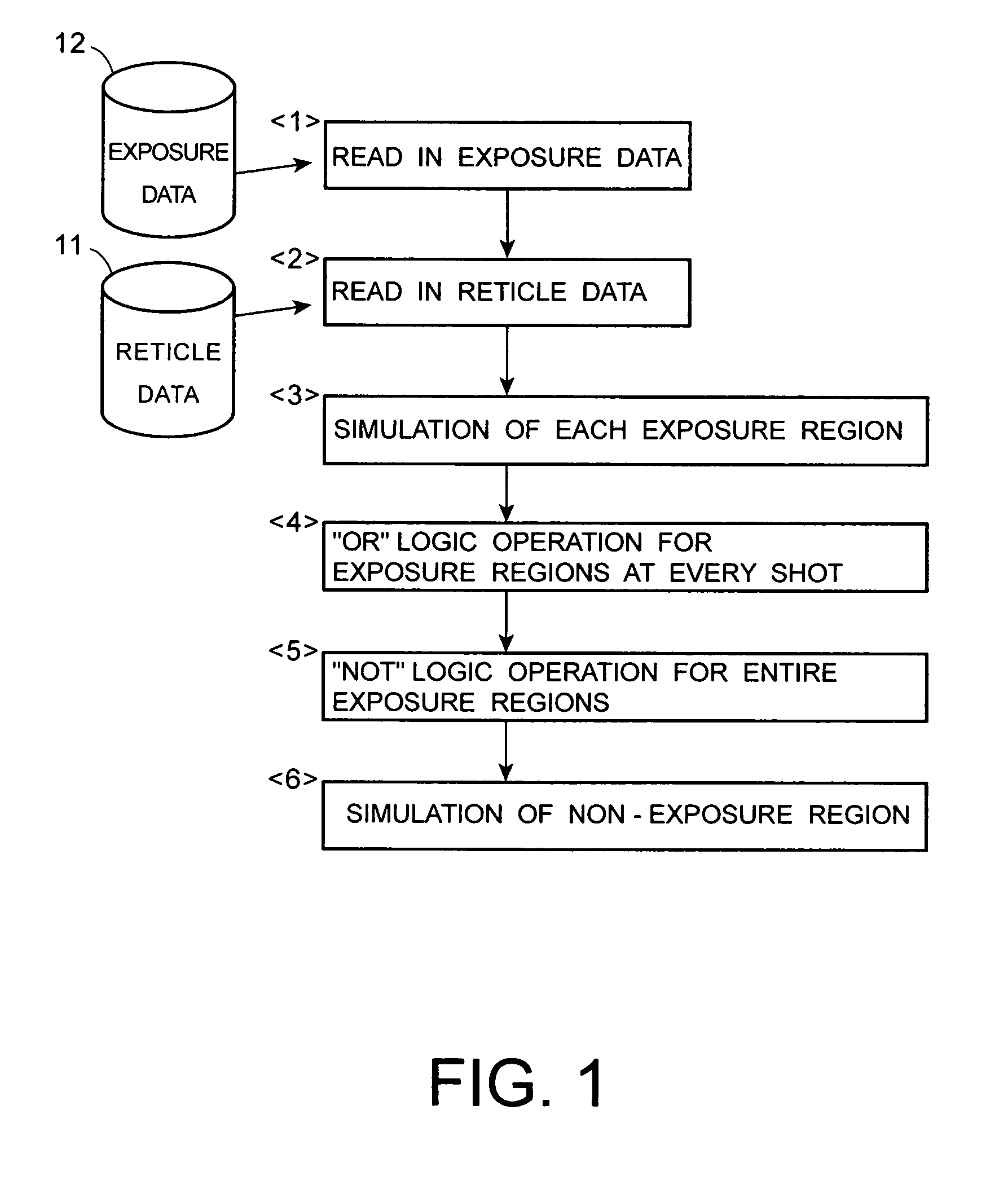
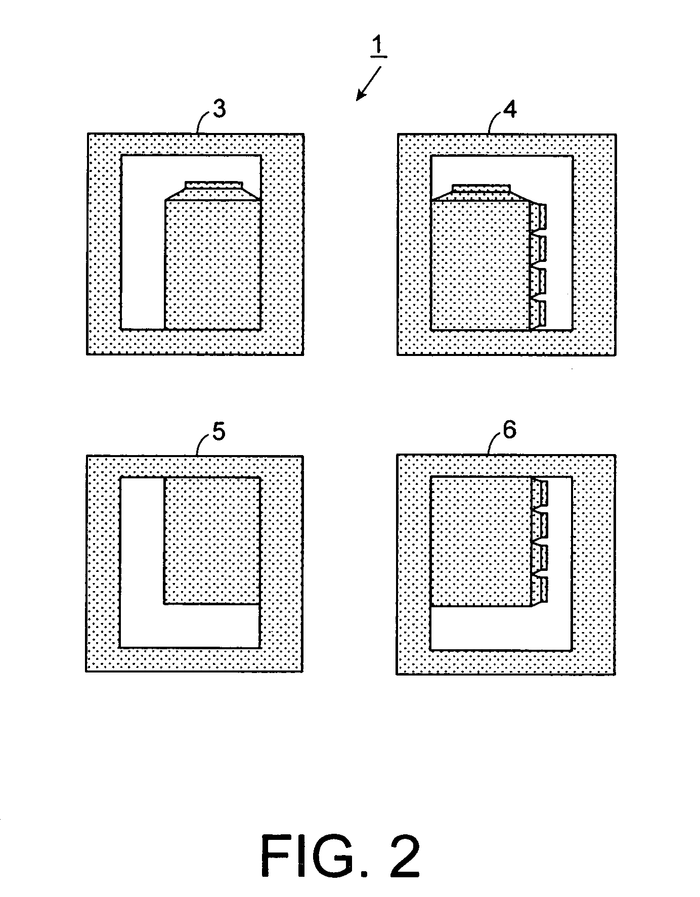
[0047]A method of simulating patterns of the present invention will be explained below with reference to FIGS. 1–6.

[0048]A manufacturing method of LCD panels is briefly outlined to begin with. As shown in FIGS. 2 and 3, reticle patterns 1 contain a plurality of reticles, e.g., four reticles in this embodiment; the first-fourth reticles 3–6 used for divided exposures of LCD panels 8 formed on a glass substrate 7. LCD panels 8 exposed through the reticle patterns 1 are further developed and etched.

[0049]The glass substrate 7 is a 400 mm×500 mm rectangular plate, for example, on which four LCD panels 8 are formed. Each LCD panel 8 includes a display region which is also a rectangle with a diagonal length of 10.4 inches in the format of XGA (Extended Graphic Adaptor: 1024×768 pixels). LCD panel 8 is provided with at least one layer made of either an electrically conductive material or a dielectric material. Exposing shots are carried out 16 times to form four LCD panels 8 on a sheet of ...

second embodiment

[0081]the present invention will be explained below with reference to FIGS. 7–9.

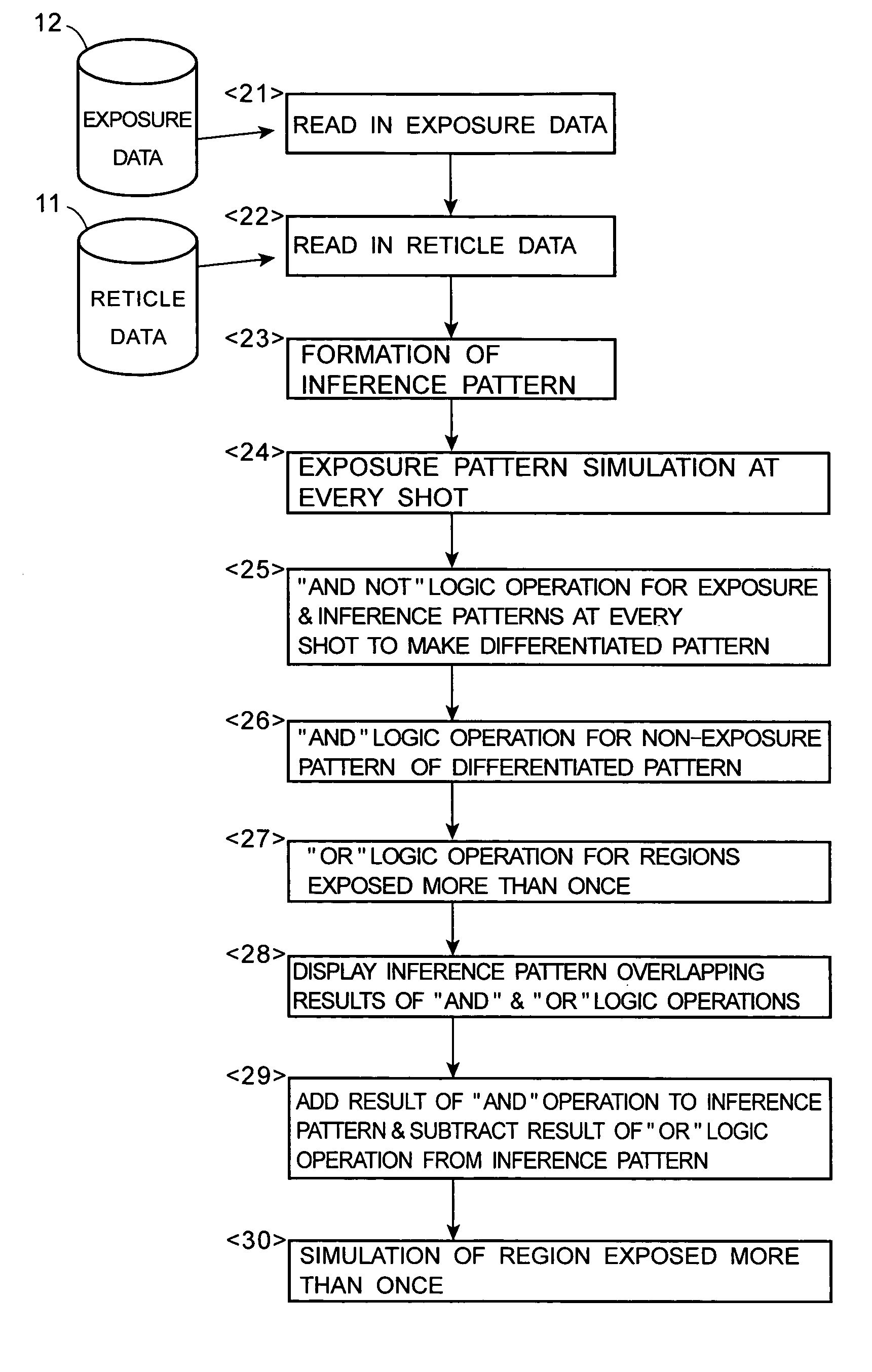
[0082]A pattern simulation method shown in FIGS. 7–9 is basically the same as that shown in FIGS. 1–6. However, a simulation computer simulates shooting exposure patterns 13 in neighboring regions on glass substrate 7 at the reversal of the first-fourth reticles 3–6 of reticle patterns 1 based on reticle data 11 and exposure data 12 and executes an AND logic operation for them so that light-shielding regions corresponding to those on glass substrate 7 which are not exposed through the first-fourth reticles 3–6 can be displayed on the monitor.

[0083]More concretely, exposure data 12 read out from an exposure data file are entered into the simulation computer (Step 11>) by reading in, and reticle data 11 are also read in by the computer (Step 12>). The computer simulates shooting exposure pattern 13 per shot on glass substrate 7 when a substrate pattern is formed on glass substrate 7 on simulation basis in ...

third embodiment

[0092]Subsequently, another AND logic operation is collectively executed for patterns corresponding to those exposed through the first-fourth reticles 3–6, respectively. As a result, computer simulation photomasks can be verified satisfactorily with those AND logic operations executed for patterns that are subject to four shots (exposures). Generally, it is quite important for a verification tool by pattern processing operations, such as a presently main stream hierarchy type verification system, to reduce operation times and a processing period of time even in a large scale pattern processing case. the present invention complies with such requirements.

[0093]Further, when exposures are carried out through the first-fourth reticles 3–6 of each LCD panel 8 divided in horizontal and vertical directions on glass substrate 7, two exposure regions arranged in diagonal places among exposure regions 15 through 18 are in contact with each other at one point which is subject to multiple expos...


PUM


Abstract

A pattern simulation method includes reticle data and exposure data. The reticle data contain reticle patterns for regions into which an entire pattern is divided. The exposure data are composed of positioning data for reticle patterns to be exposed on a substrate. A substrate pattern is formed on the substrate in accordance with the reticle data and the exposure data. OR logic operations are executed for patterns corresponding to regions of the substrate pattern exposed on the substrate to simulate exposure patterns on the substrate. Design defects of the reticle data or the exposure data can be easily found by checking of simulation patterns corresponding to regions which are not exposed on the substrate when the substrate pattern is formed on the substrate in accordance with the reticle data and the exposure data.

Description

FIELD OF THE INVENTION[0001]This invention generally relates to a method of simulating patterns formed on a substrate by applying lithographic exposure, its computer program, a medium for storing the program, and a pattern-simulation apparatus.[0002]This application is based upon and claims the benefit of priority from the prior Japanese Patent Application No. 2003-32602, filed on Feb. 10, 2003, the entire contents of which are incorporated herein by reference.BACKGROUND OF THE INVENTION[0003]In general, a liquid crystal display (“LCD”) device contains wiring such as scanning and signal lines, pixel electrodes, and switching elements such as thin film transistors. In order to make the wiring, electrodes and switching elements, thin films of conductive and dielectric materials are first formed on a substrate in a film-forming process. The thin films are then coated with a photoresist in a coating process. The coated thin films are optically exposed through patterned reticles in an ex...

Claims


Application Information

Patent Timeline
IPC IPC(8): G06F17/50G06F9/455G02F1/133G02F1/1362G03F1/00G03F7/20G06F17/00
CPCG03F7/70466G03F1/144G02F2001/13625G03F1/00G02F1/13625G01D11/26G01F1/07G01F15/10
Inventor KASHIMOTO, NOBORUITSUKI, YOSHIHARU
Owner JAPAN DISPLAY CENT INC
Learn More