Processor with demand-driven clock throttling power reduction

a clock throttling and processor technology, applied in the direction of instruments, liquid/fluent solid measurement, generating/distributing signals, etc., can solve the problems of increasing chip power consumption, increasing cooling and packaging costs, and increasing power consumption of a given clock unit, so as to reduce processor power consumption and achieve the effect of reducing performance loss without appreciable loss

Inactive Publication Date: 2006-07-11
INT BUSINESS MASCH CORP
View PDF13 Cites 38 Cited by
  • Summary
  • Abstract
  • Description
  • Claims
  • Application Information

AI Technical Summary

Benefits of technology

[0016]It is a purpose of the present invention to reduce processor power consumption, without appreciable performance loss.

Problems solved by technology

Generally, the power consumed by a given clocked unit increases linearly with the frequency of switching within it Thus, not withstanding the decrease of chip supply voltage, chip power consumption has increased as well.
Both at the chip and system levels cooling and packaging costs have escalated as a natural result of this increase in chip power.
Thus, the increase in microprocessor power dissipation has become a major stumbling block for future performance gains.
However, bus and off-chip memory speeds have not kept pace with processor computing logic core.
This can save a considerable amount of chip power.
There are at least two problems arising from coarse idle control that must be addressed.
First, large transient current drops and gains can cause unacceptable levels of inductive (Ldi / dt) noise in on-chip supply voltage.
Second, overhead cycles are required for gating off and on processes to maintain correct functional operation.
Switch between gated and enabled modes too frequently for finer grain phase changes in the workload, results in an unacceptable performance hit.
These state of the art approaches do not generate the gating signal on a predictive or anticipatory basis.
726–731, (June 1998) discuss how these constraints can significantly complicate design timing analysis, even resulting in a degraded clock-frequency performance.

Method used


Image

  • Processor with demand-driven clock throttling power reduction
  • Processor with demand-driven clock throttling power reduction
  • Processor with demand-driven clock throttling power reduction

Examples


Embodiment Construction

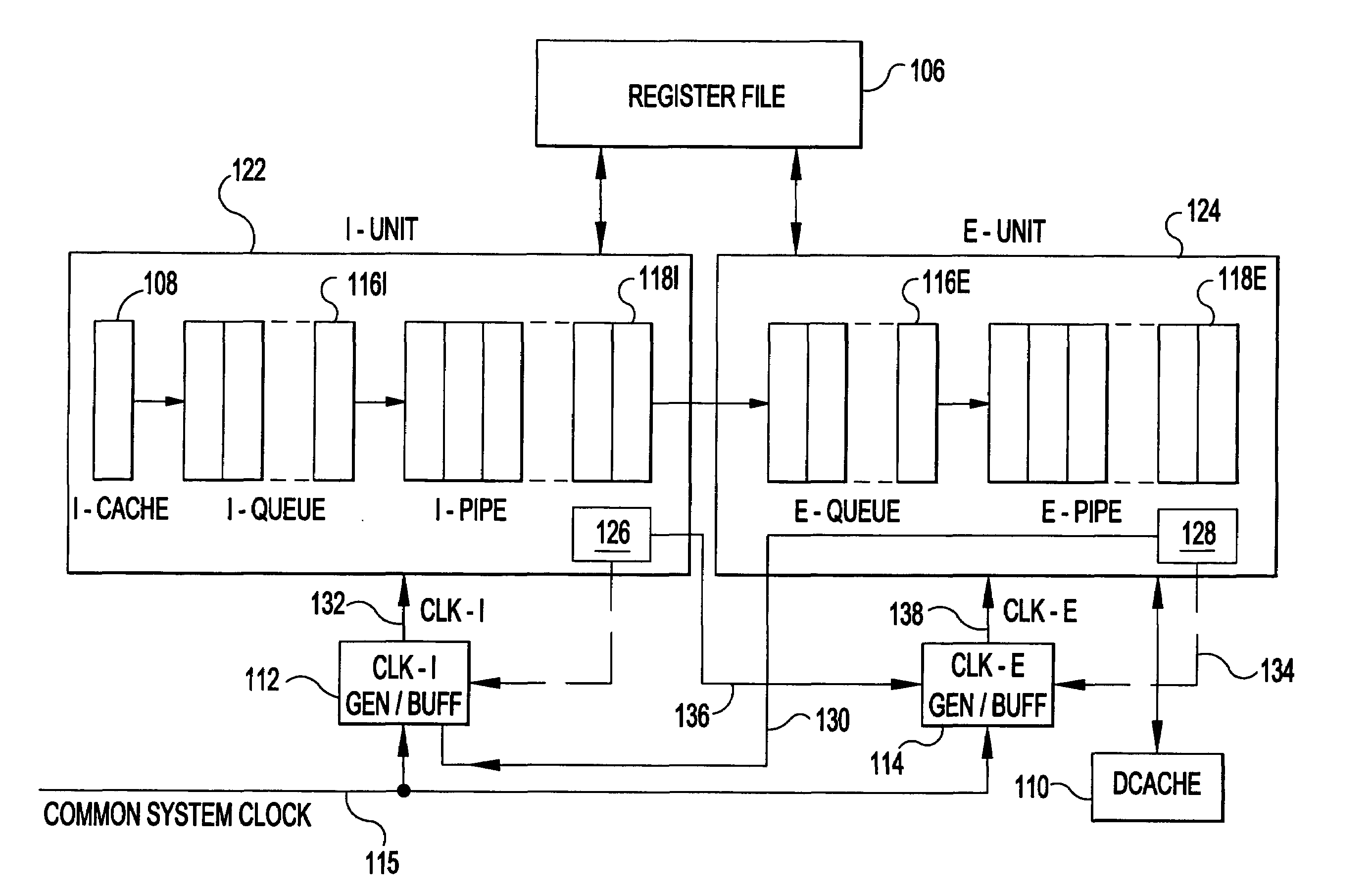
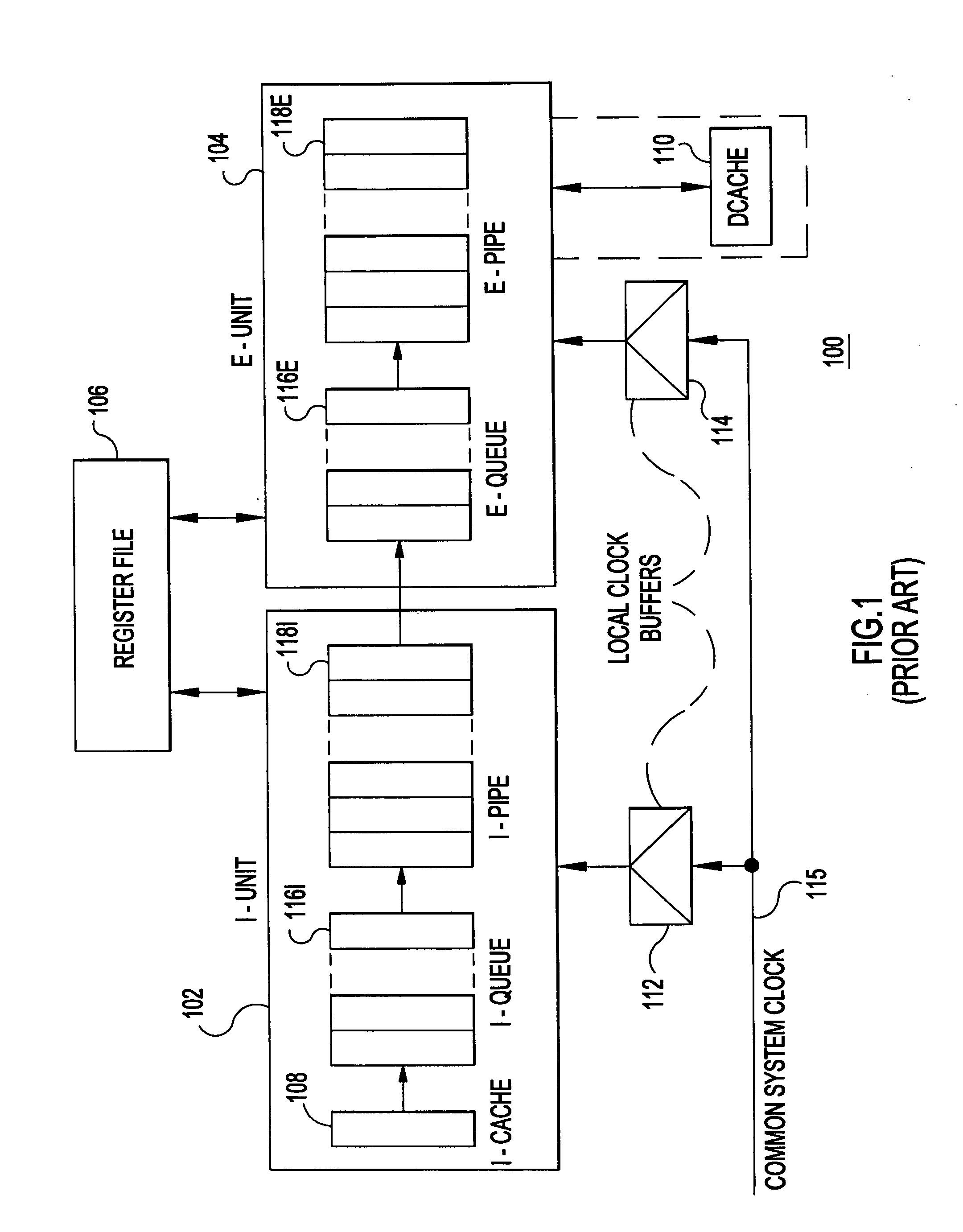
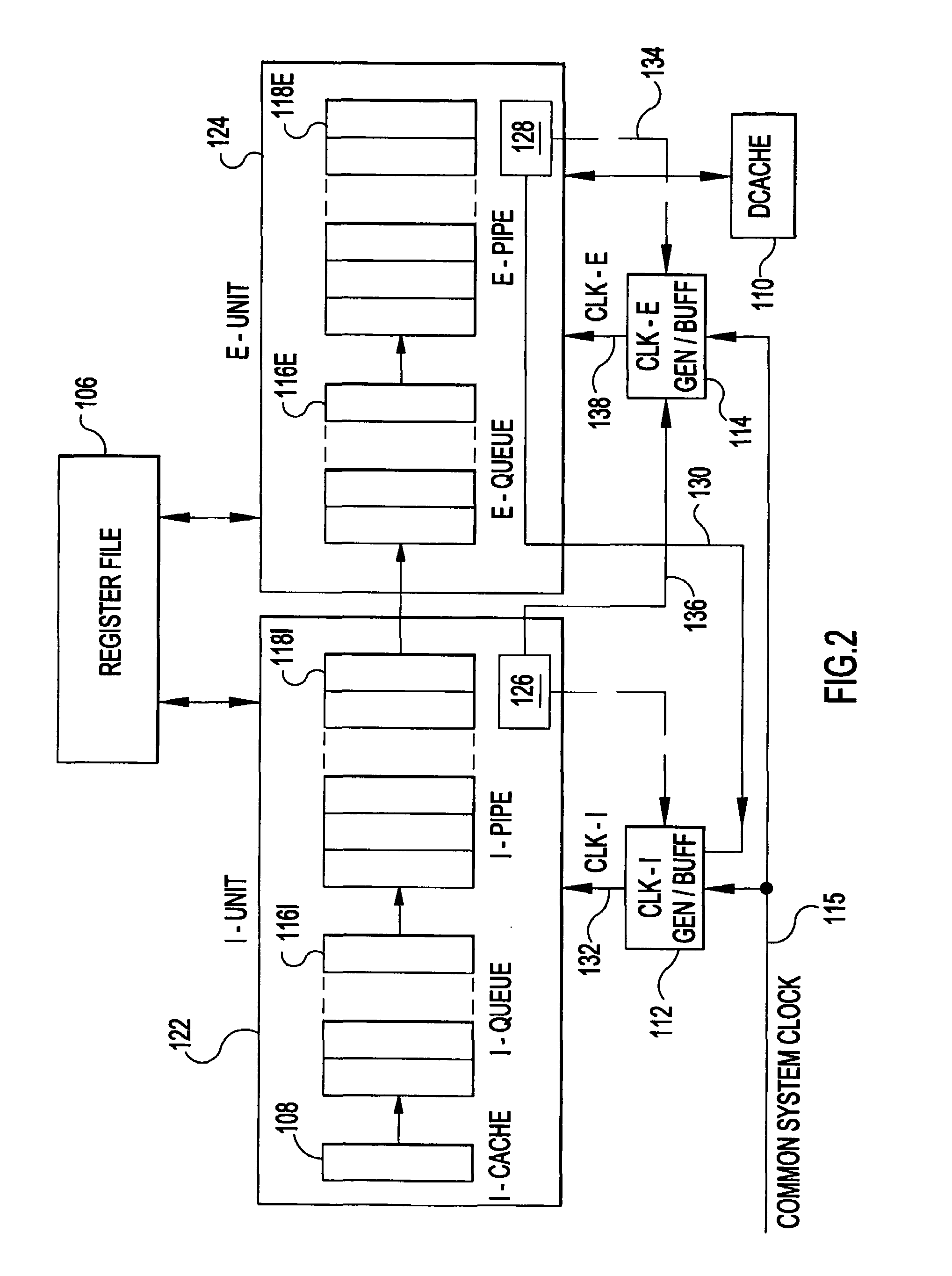
[0027]Turning now to the drawings and, more particularly, FIG. 1 shows a high level block diagram example of a typical state of the art pipelined scalar processor 100 and a corresponding instruction timing diagram. The main functional data path is divided into two major components or units, normally called the instruction unit (I-UNIT) 102 and the execution unit (E-UNIT) 104. Many detailed sub-units and functional logic, e.g., branch prediction logic, within the I-UNIT 102 and E-UNIT 104 are not germane to discussion of the present invention and so, are omitted for clarity of description of the overall clock control in such a processor 100. The processor 100 of this example is representative of a pipelined scalar design that does not include clock-gating to prevent redundant clocking of units, sub-units or attendant storage resources contained therein.

[0028]On-chip storage accessed by one or both units 102, 104 include register file (REGFILE) 106, instruction cache (ICACHE) 108 and ...


PUM


Abstract

A synchronous integrated circuit such as a scalar processor or superscalar processor. Circuit components or units are clocked by and synchronized to a common system clock. At least two of the clocked units include multiple register stages, e.g., pipeline stages. A local clock generator in each clocked unit combines the common system clock and stall status from one or more other units to adjust register clock frequency up or down.

Description

BACKGROUND OF THE INVENTION[0001]1. Field of the Invention[0002]The present invention generally relates to the reduction and control of power consumption in a microprocessor or system comprised of a plurality of clocked components or units.[0003]2. Description of the Related Art[0004]Semiconductor technology and chip manufacturing advances have resulted in a steady increase of on-chip clock frequencies, the number of transistors on a single chip and the die size itself and a corresponding increase in chip supply voltage. Generally, the power consumed by a given clocked unit increases linearly with the frequency of switching within it Thus, not withstanding the decrease of chip supply voltage, chip power consumption has increased as well. Both at the chip and system levels cooling and packaging costs have escalated as a natural result of this increase in chip power. At the low end for systems (e.g., handhelds, portable and mobile systems), where battery life is crucial, net energy re...

Claims


Application Information

Patent Timeline
Patent Type & Authority Patents(United States)
IPC IPC(8): G06F1/04G06F1/32G06F9/38
CPCG06F1/04G06F9/384G06F1/3237G06F1/324G06F1/3243G06F1/3287G06F9/30083G06F9/3802G06F9/3836G06F9/3867G06F9/3869G06F1/3203Y02B60/1217Y02B60/1221Y02B60/1239Y02B60/1282Y02D10/00
Inventor BOSE, PRADIPCITRON, DANIEL M.COOK, PETER W.EMMA, PHILIP G.JACOBSON, HANS M.KUDVA, PRABHAKAR N.SCHUSTER, STANLEY E.RIVERS, JUDE A.ZYUBAN, VICTOR V.
Owner INT BUSINESS MASCH CORP
Why Eureka
Try Eureka