Bubbler for substrate processing

a substrate and bubbler technology, applied in the field of trisilane and si3h8, to achieve the effect of improving the deposition process and high quality

Active Publication Date: 2006-07-18
ASM IP HLDG BV
View PDF26 Cites 65 Cited by
  • Summary
  • Abstract
  • Description
  • Claims
  • Application Information

AI Technical Summary

Benefits of technology

[0011]Methods have now been discovered that utilize trisilane to deposit high quality Si-containing films over a variety of substrates. See, e.g., U.S. Patent Applications (i) IMPROVED PROCESS FOR DEPOSITION OF SEMICONDUCTOR FILMS, Ser. No. 10 / 074,563, filed Feb. 11, 2002, (ii) DOPANT PRECURSORS AND PROCESSES, Ser. No. 10 / 074,149, filed Feb. 11, 2002, (iii) INTEGRATION OF HIGH K GATE DIELECTRIC, Ser. No. 10 / 074,722, filed Feb. 11, 2002, (iv) DEPOSITION OVER MIXED SUBSTRATES, Ser. No. 10 / 074,633, filed Feb. 11, 2002, (v) THIN FILMS AND METHODS OF MAKING THEM, Ser. No. 10 / 074,564, filed Feb. 11, 2002, and (vi) IMPROVED PROCESS FOR DEPOSITION OF SEMICONDUCTOR FILMS, Ser. No. 10 / 074,534, filed Feb. 11, 2002, which are hereby incorporated by reference herein in their entireties. However, implementing such methods into a commercially viable substrate processing apparatus creates several engineering challenges.

Problems solved by technology

However, implementing such methods into a commercially viable substrate processing apparatus creates several engineering challenges.

Method used


Image

  • Bubbler for substrate processing
  • Bubbler for substrate processing
  • Bubbler for substrate processing

Examples


example 1

[0094]An eight-inch diameter (200 mm) silicon wafer substrate having a 1,000 Å SiO2 layer was placed into the reactor chamber and allowed to reach thermal equilibrium at 450° C. at 40 Torr pressure under a flow of 20 standard liters per minute (slm) of high purity hydrogen gas. Trisilane was introduced to the chamber by passing high purity hydrogen gas through liquid trisilane using a bubbler (maintained at room temperature using a water bath around the vessel containing the trisilane) connected by a feed line to the chamber. A flow rate of 180 standard cubic centimeters per minute (sccm) of the hydrogen / trisilane mixture, along with a flow of 90 sccm (inject) of diborane (100 ppm, 90 sccm mixed with 2 slm high purity hydrogen), was then passed into the reactor for four minutes. A continuous, boron-doped, amorphous silicon film having a total thickness of 56 Å and a surface roughness of about 2 Å rms (comparable to the underlying silicon dioxide) was deposited on the silicon dioxide...

example 3

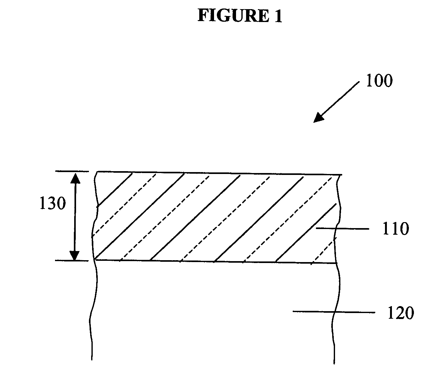
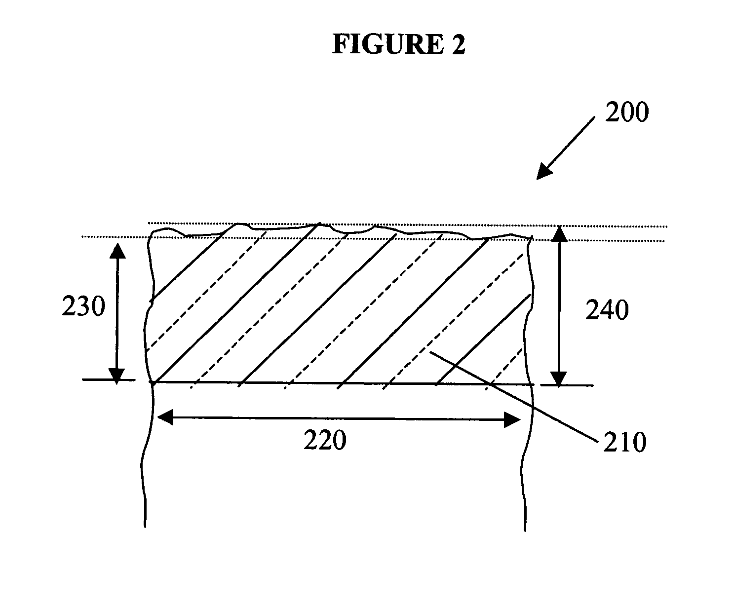
[0096]The process of Example 1 was repeated, except that the flow rate was 228 sccm, diborane was not used, and the deposition time was two minutes. A continuous amorphous silicon film having a total thickness of 28 Å and a surface roughness of about 2 Å rms (comparable to the underlying silicon dioxide) was deposited on the silicon dioxide layer at a deposition rate of 14 Å per minute. A layer of epoxy was then applied to facilitate cross-sectional sample preparation. FIG. 10 is reproduction of an electron micrograph showing a cross section of the resulting substrate showing the underlying SiO2 layer (“oxide”), the deposited amorphous silicon film (“a-Si”), and the overlying epoxy layer (“epoxy”).

example 4

[0097]An eight-inch diameter (200 mm) silicon wafer substrate having a 1,000 Å SiO2 layer was placed into the reactor chamber and allowed to reach thermal equilibrium at 600° C. at 40 Torr pressure under a flow of 20 standard liters per minute (slm) of high purity hydrogen gas. Trisilane was introduced to the chamber by passing high purity hydrogen gas through liquid trisilane using a bubbler (maintained at room temperature using a water bath around the vessel containing the trisilane) connected by a feed line to the chamber. A flow rate of 180 standard cubic centimeters per minute (sccm) of the hydrogen / trisilane mixture, along with a flow of 90 sccm (inject) of diborane (100 ppm, 90 sccm mixed with 2 slm high purity hydrogen), was then passed into the reactor for 15 seconds to deposit an amorphous boron-doped silicon film having a thickness of 100 Å. Under these conditions, the delivery rate of trisilane to the substrate was about 0.1 gram per minute. The deposition rate was 400 ...


PUM


Abstract

A vaporization chamber for a substrate processing system includes a main body, a cover member and a transition member. The main body is made of aluminum and defines a first inner surface, which defines, at least in part, a cavity. The cover member is also made of aluminum. The cover member defines a second inner surface, which also defines, at least in part, the cavity. The cover member includes a carrier gas cover inlet, a liquid source cover inlet, a source cover outlet which extends from a first outer surface through the cover member to the second inner surface. The transition member is made of stainless steel and has a transition outer surface and a transition inner surface. The transition inner surface is aluminum cladded. The cover member includes a carrier gas cover inlet, a liquid source cover inlet, a source cover outlet which extend from a first outer surface through the cover member to second inner surface. The transition inner surface and the cover outer surface are welded together.

Description

PRIORITY INFORMATION[0001]This application claims the priority benefit under 35 U.S.C. § 119(e) of Provisional Application 60 / 398,073 filed Jul. 23, 2002 and Provisional Application 60 / 397,806 filed Jul. 19, 2002.BACKGROUND OF THE INVENTION[0002]1. Field of the Invention[0003]This invention relates generally to the deposition of silicon-containing films, and more particularly to the use of trisilane, Si3H8, in chemical vapor deposition processes for the deposition of thin silicon-containing films on various substrates.[0004]2. Description of the Related Art[0005]Silane (SiH4) is widely used in the semiconductor manufacturing industry to deposit silicon-containing (“Si-containing”) films by chemical vapor deposition (CVD). However, the deposition of very thin (e.g., about 150 Å or less) silicon-containing films using silane is very challenging, particularly over large area substrates. Very thin Si-containing films deposited using silane are often not continuous, due to island-like fi...

Claims


Application Information

Patent Timeline
Patent Type & Authority Patents(United States)
IPC IPC(8): B01F3/04C23C16/24C23C16/40C23C16/448H01L21/02H01L21/205
CPCC23C16/24C23C16/402C23C16/4482Y10S261/65H01L28/84
Inventor STAMP, MICHAEL R.AMRHEIN, FREDERICK J.DALE, ARNOLD J.POTTEBAUM, JOSEPH C.EBERT, BRIAN J.
Owner ASM IP HLDG BV
Why Eureka
Try Eureka