
Method for controlling etch process repeatability

a repeatability control and etching technology, applied in the field of semiconductor device fabrication processes, can solve the problems of reduced budgets, reduced void-free filling of narrow width, and sometimes closing of the top part of a high aspect ratio structure, so as to reduce or eliminate chamber loading and redeposition, and improve the uniformity of wafer-to-wafer. uniform

Active Publication Date: 2006-07-18
NOVELLUS SYSTEMS
View PDF54 Cites 158 Cited by
  • Summary
  • Abstract
  • Description
  • Claims
  • Application Information

AI Technical Summary

Benefits of technology

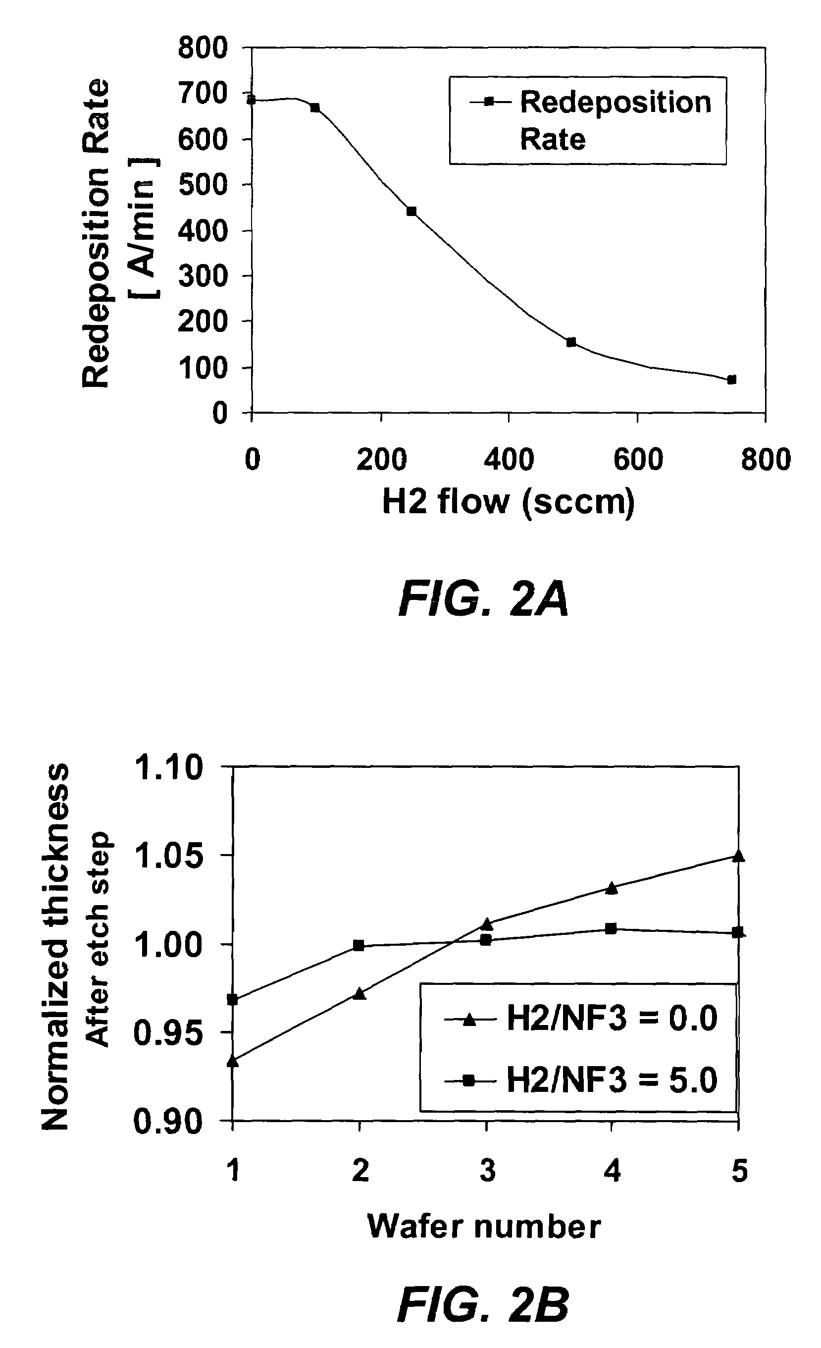
[0008]The present invention addresses this need by providing plasma etch processes incorporating etch chemistries which include hydrogen. In particular, the invention provides high density plasma chemical vapor deposition-etch-deposition processes incorporating etch chemistries which include hydrogen that can effectively fill high aspect ratio (typically at least 3:1, for example 6:1, and up to 10:1 or higher), narrow width (typically sub 0.13 micron, for example 0.1 micron or less) gaps while reducing or eliminating chamber loading and redeposition and improving wafer-to-wafer uniformity relative to conventional deposition-etch-deposition processes which do not incorporate hydrogen in their etch chemistries.
[0011]Suitable plasma reactors with inductively coupled plasma (ICP) sources are available to accomplish both of these deposition and etch techniques in a single plasma reactor chamber. Conducting all deposition and etch processes in a single plasma reactor chamber increases throughput and reduces handling of wafers resulting in more efficient and higher quality gap fill operations.
[0013]In another aspect, the invention pertains to a method of etching and minimizing the redeposition of gapfill materials on a partially filled gap on a semiconductor substrate. The method involves partially removing dielectric deposited in the gap from the gap opening by an etch back process and reducing the film removal from the chamber wall conducted with process chemistry including hydrogen.

Problems solved by technology

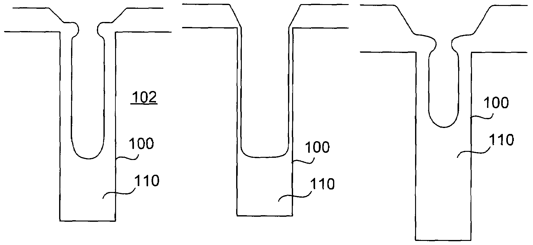
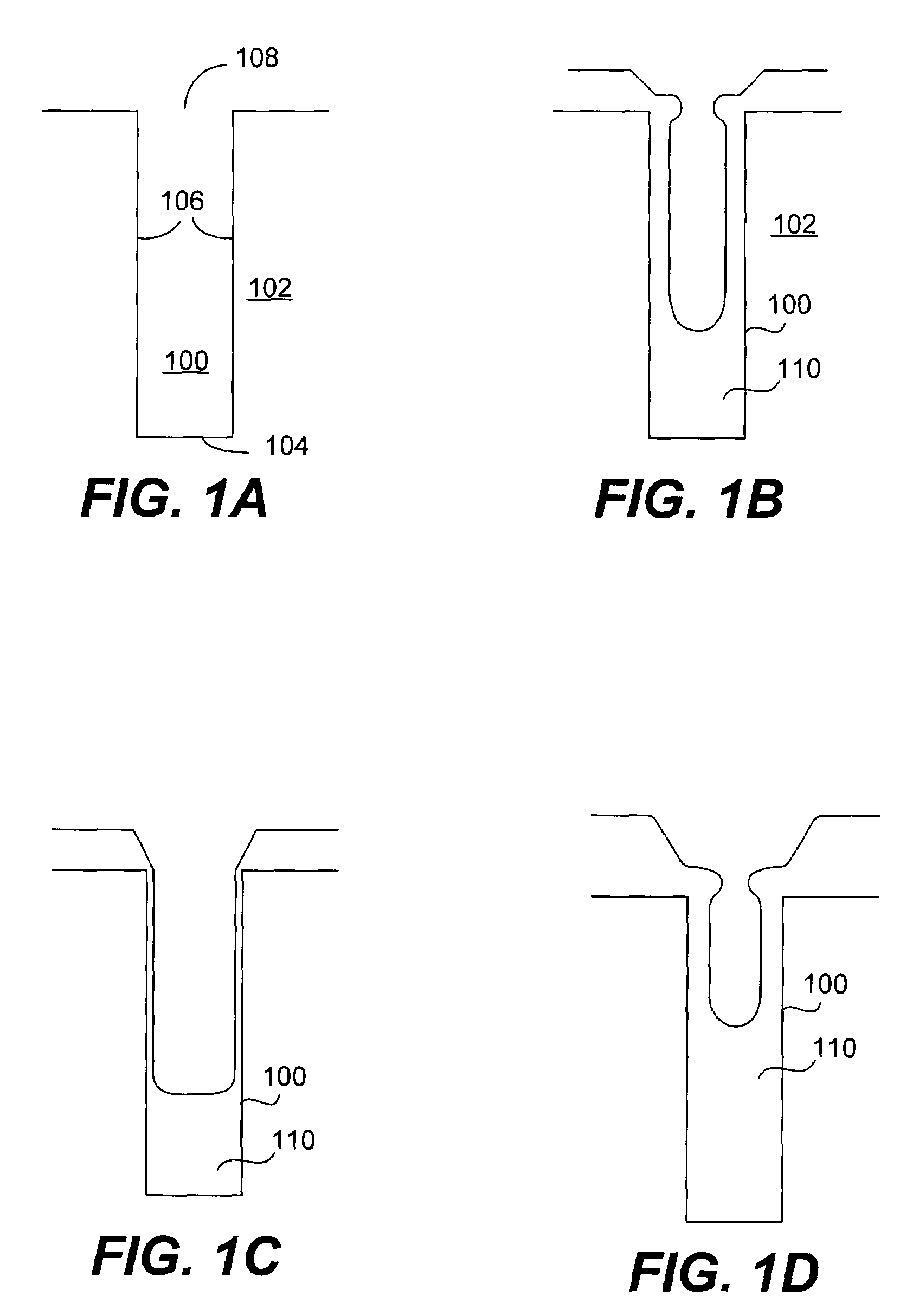
As device geometries shrink and thermal budgets are reduced, void-free filling of narrow width, high aspect ratio spaces (e.g., AR>3:1) becomes increasingly difficult due to limitations of existing deposition processes.
As a result the top part of a high aspect ratio structure sometimes closes prematurely leaving voids within the gap's lower portions.
This problem is exacerbated in small features.
Furthermore, as aspect ratios increase, the shape of the gap itself can contribute to the problem.
High aspect ratio gaps often exhibit reentrant features, which make gap filling even more difficult.
The most problematic reentrant feature is a narrowing at the top of the gap; the etched side-walls slope inward near the top of the gap.
Hence voids and seams become even more likely.
Thus, HDP CVD is not an entirely diffusion-based (isotropic) process.
The etch process is susceptible to a “loading effect,” such that etch process response on each successive wafer processed in a reactor is a function of the loading condition of the reactor.
This “loading effect” phenomena leads to a wafer-to-wafer process repeatability issue with dep-etch-dep processes thus limiting the proliferation of this technique despite its superior gap fill capability.

Method used


Image

  • Method for controlling etch process repeatability
  • Method for controlling etch process repeatability
  • Method for controlling etch process repeatability

Examples


Embodiment Construction

[0022]Reference will now be made in detail to specific embodiments of the invention. Examples of the specific embodiments are illustrated in the accompanying drawings. While the invention will be described in conjunction with these specific embodiments, it will be understood that it is not intended to limit the invention to such specific embodiments. On the contrary, it is intended to cover alternatives, modifications, and equivalents as may be included within the spirit and scope of the invention as defined by the appended claims. In the following description, numerous specific details are set forth in order to provide a thorough understanding of the present invention. The present invention may be practiced without some or all of these specific details. In other instances, well known process operations have not been described in detail in order not to unnecessarily obscure the present invention.

[0023]Introduction

[0024]The present invention relates to chemical vapor deposition and e...


PUM

PropertyMeasurementUnit
pressureaaaaaaaaaa
temperatureaaaaaaaaaa

Abstract

Plasma etch processes incorporating etch chemistries which include hydrogen. In particular, high density plasma chemical vapor deposition-etch-deposition processes incorporating etch chemistries which include hydrogen that can effectively fill high aspect ratio (typically at least 3:1, for example 6:1, and up to 10:1 or higher), narrow width (typically sub 0.13 micron, for example 0.1 micron or less) gaps while reducing or eliminating chamber loading and redeposition and improving wafer-to-wafer uniformity relative to conventional deposition-etch-deposition processes which do not incorporate hydrogen in their etch chemistries.

Description

BACKGROUND OF THE INVENTION[0001]This invention relates to semiconductor device fabrication processes. More specifically, the invention relates to plasma-based chemical vapor deposition and etch processes for forming dielectric layers, particularly in high aspect ratio, narrow width recessed features.[0002]It is often necessary in semiconductor processing to fill high aspect ratio gaps with insulating material. This is the case for shallow trench isolation, inter-metal dielectric layers, passivation layers, etc. As device geometries shrink and thermal budgets are reduced, void-free filling of narrow width, high aspect ratio spaces (e.g., AR>3:1) becomes increasingly difficult due to limitations of existing deposition processes.[0003]Most deposition methods either deposit more material on the upper region than on the lower region of a side-wall or form cusps at the entry of the gap. As a result the top part of a high aspect ratio structure sometimes closes prematurely leaving void...

Claims


Application Information

Patent Timeline
Patent Type & Authority Patents(United States)
IPC IPC(8): H01L21/76
CPCC23C16/045C23C16/401H01L21/02164H01L21/31116H01L21/31612H01L21/76224H01L21/02274Y10S438/959
Inventor SUTANTO, SISWANTOZHU, WENXIANFUNG, WAIKITLIM, MAYASARIGAURI, VISHALPAPASOULIOTIS, GEORGE D.
Owner NOVELLUS SYSTEMS
Learn More