Contact structures and methods for making same

a contact structure and contact technology, applied in the field of electronic assemblies and testing, can solve the problems of high-speed wirebonding equipment that the reaction between copper and solder at elevated temperatures is undesirable, and the high-speed wirebonding equipment cannot handle a 30 mil diameter wire, etc., to achieve the effect of low cost and high volum

Inactive Publication Date: 2006-08-01
FORMFACTOR INC
View PDF277 Cites 3 Cited by
  • Summary
  • Abstract
  • Description
  • Claims
  • Application Information

AI Technical Summary

Benefits of technology

[0021]One object of the present invention is to provide a high volume, low cost manufacturing process for production of precise shape and geometry protuberant conductive contacts on a wide variety of electronic components, the contacts having a controlled set of physical, metallurgical and mechanical properties, bulk and surface. Such protuberant contacts can be employed to satisfy electrical, thermal or geometrical requirements in various aspects of electronic interconnection applications. An inventive, multiple stage process is provided, according to which, first, wire stems are bonded to contact carrying terminals, the stems being shaped in three dimensional space, to define skeletons of the resulting contacts. The conductive contacts are then completed through at least one deposition step of a coating which envelopes or jackets the wire skeletons and the terminals. The common coating not only helps to “anchor” protruding contacts to the terminals, but also provides for characteristics of the protuberant contacts with respect to long term stability of their engagement contact with mating electronic component, including but not limited to interconnection substrates, semiconductor devices, interconnect or test sockets. The coating also determines soldering assembly characteristics, as well as long term effects from contact with solder. The coating, along with the wire material properties, determines the mechanical characteristics of the resulting protuberant, contact. The wire serves as a “skeleton” of a resulting protruding contact, and the coating serves as its. “muscle”.
[0023]An additional object of the present invention is to produce array patterns of contacts for unique component designs, without incurring costs and delays associated with production of unique tooling. This object is achieved through use of a sequential wirebonding process for attaching of the wire skeletons to the terminals, and then overcoating them in a single, non-pattern-specific step. Location targeting and geometric characteristics are entered into an electronic control system of the wirebonding equipment with a specific set of commands. A program controls all aspects of wire forming and shaping process, as well as bond characteristics. Production of the multiple protruding contacts does not require time-limiting and costly production of molds, masks or the like, which otherwise would be specific to every incoming order. This object is exemplified by application of the present invention to production of integrated pin-shaped contacts for ceramic pin grid array packages. This is achieved by bonding straight vertical, single stem skeletons, perpendicular to the surface of terminals, and overcoating them with a conductive structural metal or alloy, consisting substantially of nickel, copper, cobalt, iron or alloys thereof, with the thickness of the deposit determined by the required pin diameter value. This can also be accomplished with equal ease on plastic pin carrying substrates.
[0024]Yet another object of the present invention is to create protruding, tower-like solder contacts which substantially maintain a well controlled aspect ratio even when the solder is molten. This object is achieved through first bonding a wire skeleton which will define the final shape and aspect ratio of a solder contact, then optionally overcoating it with a barrier layer which prevents long term reaction between the solder and the wire, and finally depositing a mass of solder which wets the skeleton with a barrier, and clings onto the skeleton even after multiple reflows.

Problems solved by technology

The polymer coating, which is optional, also compensates for another disadvantage of the approach, namely weak points along the wire, typically the point of contact between the wire and terminal metallization, and in case of ball bonding, in a heat effected zone of the wire just above impression of a bonding capillary.
For instance, standard, high speed wirebonding equipment could not handle a 30 mil diameter wire.
Therefore, according to these inventions, a 30 mil diameter, 100 mil high contact could only be produced on lower throughput specialized equipment, at higher cost.
In addition, a gold wire as described in a preferred embodiment, would have a problem of dissolving in solder during a soldering cycle, which causes long term reliability problems with solder joints similarly, direct soldering of copper contacts would in many cases result in undesirable reaction between copper and solder at elevated temperatures.
While nickel metal-is the material of choice for solder joint reliability, nickel wire can not be used for ultrasonic wirebonding to metal terminals due to its high mechanical strength and passivating, oxide forming properties.
This approach is incapable of producing high aspect ratio protruding contacts because of limitations of the extrusion method.
In addition, dissolution of gold in solder, as taught by this approach creates a problem due to reliability concerns.
The method also limits selection of contact material to easily extrudable metals, like gold.
This method is only limited to contact materials which are reflowed during the assembly, and requires external hardware for forming the contact shape, which adds cost of the hardware and increases the process complexity.
This approach also requires hardware means for maintaining longitudinal dimension of the contacts, and does not lend itself to standard practices of surface mount soldering, in which industry already has made substantial time and capital investments.
This approach requires generating a mold for each solder column array pattern, commonly involving undesirable non-recurring engineering expenses and associated increase in delivery times.
Additionally, soldering usually requires flux, while the interposer material makes it difficult to clean flux after the reflow process.
This approach, as several of the above described approaches, requires a custom made retaining member for every interconnect application, and therefore requires an additional non-recurring engineering expense and increased delivery time for every production order.
While providing means for controlled aspect ratio interconnect joints, this approach also requires use of a custom manufactured interposer and inevitable non-recurring engineering expenses and increased delivery times. In addition, when improved alignment of the interconnect to the terminals is required, as terminal-to-terminal distances decrease, this approach suffers from heat and environmental effects on interposer material, causing it to distort or change dimension during processing steps, which makes the alignment difficult, and limits this approach to relatively coarse terminal-to-terminal pitch applications.
Deposition of such a structure of solder is a lengthy and expensive process.

Method used


Image

  • Contact structures and methods for making same
  • Contact structures and methods for making same
  • Contact structures and methods for making same

Examples


Embodiment Construction

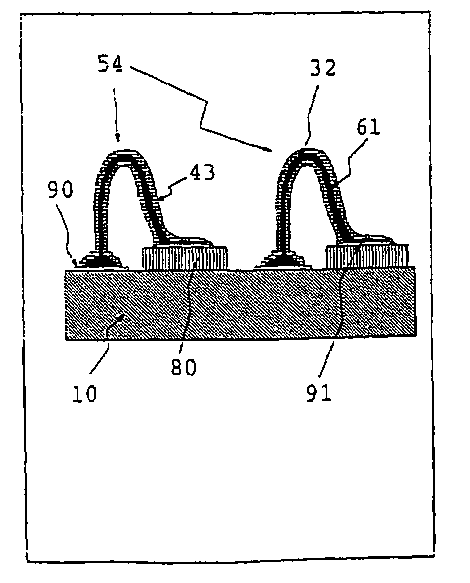
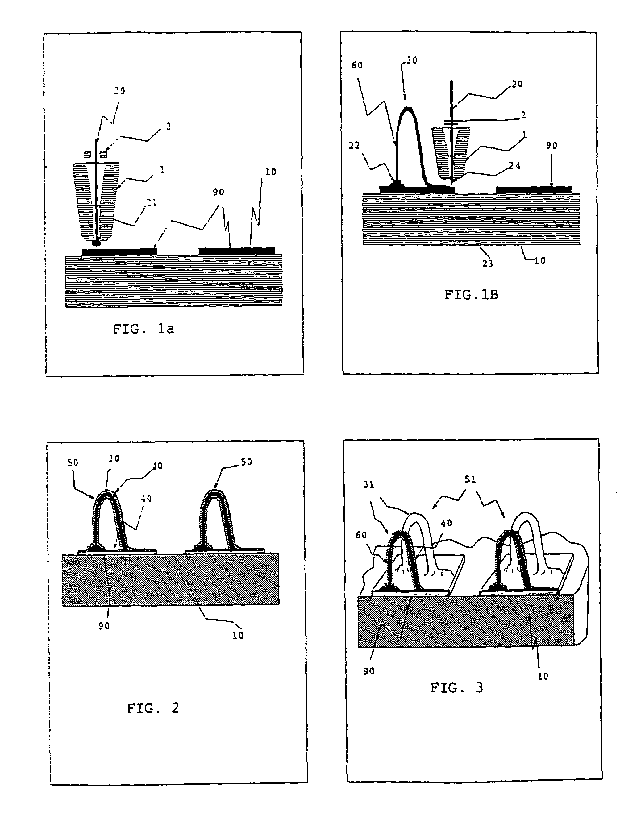
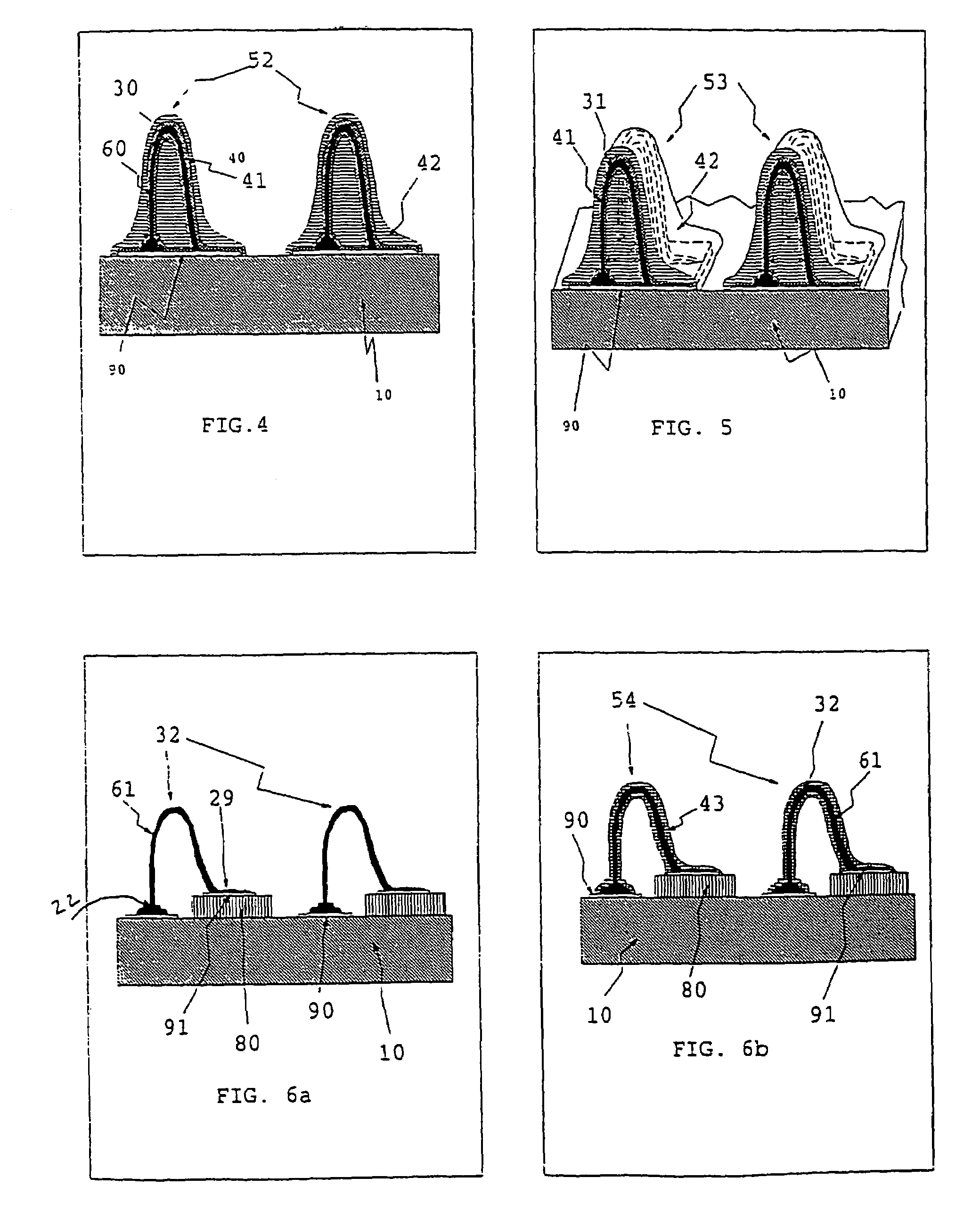
[0048]The method of the present invention relies on wirebonding equipment to produce controlled aspect ratio and shape wire skeletons, which are subsequently overcoated with a desired material in order to produce a required set of properties for protuberant electrical contacts. FIGS. 1A and 1B depict use of a ball-and-wedge wirebonding machine to form a wire skeleton. More detailed descriptions of this and wedge-wedge wirebonding methods, commonly used in the semiconductor industry for interconnecting silicon devices to packages, can be found in Electronic Packaging and Interconnection Handbook edited by Charles A. Harper, on pp. 6.62–6.64 and 7.28–7.30. FIG. 1A illustrates a capillary 1, with an open clamp 2, containing an end portion of a continuous wire 20 with a ball 21 formed at its feed end below the capillary tip. The ball 21 is brought in contact with a contact carrying terminal 90 on top of (or otherwise contained within) a substrate 10. As a result of application of pressu...


PUM

PropertyMeasurementUnit
diameteraaaaaaaaaa
diameteraaaaaaaaaa
tensile strengthaaaaaaaaaa

Abstract

Contact structures are formed by building a core structure on a substrate and over coating the core structure with a material that is harder or has a greater yield strength than the material of the core structure. The core structure may be formed by attaching a wire to the substrate and spooling the wire out from a spool. While spooling the wire out, the spool may be moved to impart a desired shape to the wire. The wire is severed from the spool and over coated. As an alternative, the wire is not over coated. The substrate may be an electronic device, such as a semiconductor die.

Description

CROSS-REFERENCE TO RELATED APPLICATIONS[0001]This application is a continuation of U.S. patent application Ser. No. 10 / 290,639, filed Nov. 7, 2002 now U.S. Pat. No. 6,818,840, which is a continuation of U.S. patent application Ser. No. 09 / 245,499, filed Feb. 5, 1999 (abandoned), which is continuation of U.S. patent application Ser. No. 08 / 457,479, filed Jun. 1, 1995 (now U.S. Pat. No. 6,049,976), which is a divisional of U.S. patent application Ser. No. 08 / 152,812, filed Nov. 16, 1993 (now U.S. Pat. No. 5,476,211).BACKGROUND OF THE INVENTION[0002]This invention relates in general to electronic assemblies and testing thereof. In particular, the invention relates to a method of manufacture of protruding, controlled aspect ratio and shape contacts for uses in interconnections of assemblies and testing thereof.[0003]Interconnections which involve protruding electrical contacts are used extensively in packaging of electronics. Pin grid array packages, both plastic and ceramic, housing a ...

Claims


Application Information

Patent Timeline
Patent Type & Authority Patents(United States)
IPC IPC(8): H01R9/00B23K1/00C23C18/16C25D7/12G01R1/04G01R1/067G01R1/073G01R3/00G01R31/28H01L21/00H01L21/48H01L21/56H01L21/60H01L21/66H01L23/48H01L23/485H01L23/49H01L23/498H01L25/065H01L25/16H05K1/14H05K3/30H05K3/32H05K3/34H05K3/36H05K3/40H05K7/10
CPCB23K1/0016C23C18/161C25D7/12G01R1/0466G01R31/2884H01L21/4853H01L21/563H01L21/6715H01L22/20H01L23/49811H01L24/11H01L24/16H01L24/72H01L24/81H01L25/0652H01L25/16H05K3/308H05K3/326H05K3/3426H05K3/4015H05K7/1069H01L24/13H01L24/29B23K2201/40G01R1/06711G01R1/06761G01R1/07307G01R3/00G01R31/2886H01L21/76897H01L24/45H01L24/48H01L2224/1134H01L2224/13099H01L2224/13111H01L2224/32225H01L2224/45015H01L2224/45124H01L2224/45139H01L2224/45144H01L2224/45147H01L2224/4554H01L2224/4556H01L2224/456H01L2224/4809H01L2224/48091H01L2224/4813H01L2224/48227H01L2224/48465H01L2224/49109H01L2224/73203H01L2224/73265H01L2224/78301H01L2224/81205H01L2224/81801H01L2224/85043H01L2224/85045H01L2224/85201H01L2224/85205H01L2924/01004H01L2924/01005H01L2924/01011H01L2924/01012H01L2924/01013H01L2924/01014H01L2924/01015H01L2924/01022H01L2924/01027H01L2924/01028H01L2924/01029H01L2924/0103H01L2924/01031H01L2924/01039H01L2924/01042H01L2924/01046H01L2924/01047H01L2924/01049H01L2924/0105H01L2924/01051H01L2924/0106H01L2924/01074H01L2924/01078H01L2924/01079H01L2924/01082H01L2924/01322H01L2924/01327H01L2924/014H01L2924/10253H01L2924/10329H01L2924/15153H01L2924/1517H01L2924/15312H01L2924/1532H01L2924/16152H01L2924/16195H01L2924/19041H01L2924/19043H01L2924/20751H01L2924/20752H01L2924/20753H01L2924/20754H01L2924/20755H01L2924/20756H01L2924/20757H01L2924/20758H01L2924/20759H01L2924/2076H01L2924/30107H01L2924/3011H01L2924/3025H05K1/141H05K3/3421H05K3/368H05K3/4092H05K2201/0397H05K2201/068H05K2201/1031H05K2201/10318H05K2201/10378H05K2201/10719H05K2201/10734H05K2201/10757H05K2201/10878H05K2201/10909H05K2201/10946H01L2924/0132H01L24/49H01R12/52H01L2924/01024H01L2924/01033H01L2924/01044H01L2924/01045H01L2924/19107H01L2924/00013Y10T29/49149Y10T29/49144Y10T29/49147Y10T29/49224Y10T29/49151Y10T29/49179Y10T29/49609Y10T29/49155Y10T29/49222Y10T29/49204Y10T29/49174H01L2924/00014H01L2924/00H01L2924/00012H01L2924/3512H01L2224/29099B23K2101/40H01L2924/15787H01L2224/45109H01L2224/45111H01L2224/45116H01L2224/45117H01L2224/4512H01L2224/45138H01L2224/45155H01L2224/45164H01L2224/45169H01L2224/45173H01L2224/45123H01L2224/45176H01L2224/45163H01L2224/10145H01L2224/10126Y02P70/50C25D7/123H01L2924/00015H01L2924/2075H01L2924/0102
Inventor KHANDROS, IGOR Y.
Owner FORMFACTOR INC
Why Eureka
Try Eureka