Nitride based semiconductor device

a technology of nitride and semiconductors, applied in semiconductor devices, lasers, semiconductor lasers, etc., can solve the problems of reducing the recombination efficiency between electrons and holes, deteriorating the luminous efficiency of optical devices, etc., and achieves the effect of alleviating the piezoelectric field effect and high efficiency

Active Publication Date: 2006-08-01
SAMSUNG ELECTRONICS CO LTD
View PDF2 Cites 437 Cited by
  • Summary
  • Abstract
  • Description
  • Claims
  • Application Information

AI Technical Summary

Benefits of technology

[0011]Therefore, the present invention has been made in view of the above problems, and it is an object of the present invention to provide a high efficiency nitride based semiconductor device having alleviated piezoelectric field effects by forming an electron emitting layer of a multi-structure for tunneling effects, between an active layer and n-type clad layer while controlling an energy band gap size of each layer.

Problems solved by technology

However, the above-mentioned method still suffers from a problem of lowering recombination efficiency between electrons and holes due to piezoelectric field.
Therefore, even though the effective mass of carrier injected increases, the recombination probability between electrons and holes does not substantially increase, thus leading to deterioration of luminous efficiency of the optical device.

Method used


Image

  • Nitride based semiconductor device
  • Nitride based semiconductor device
  • Nitride based semiconductor device

Examples


example 1

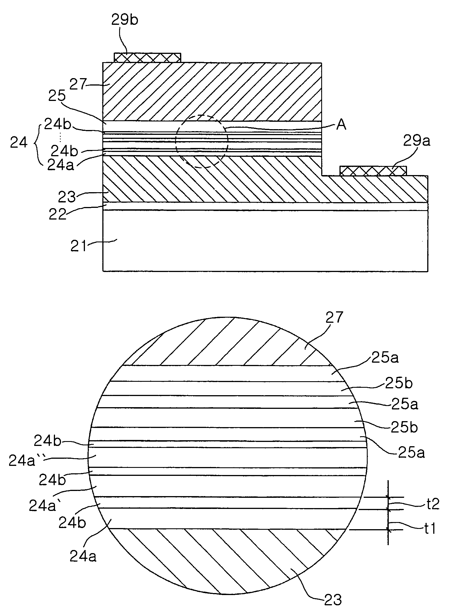
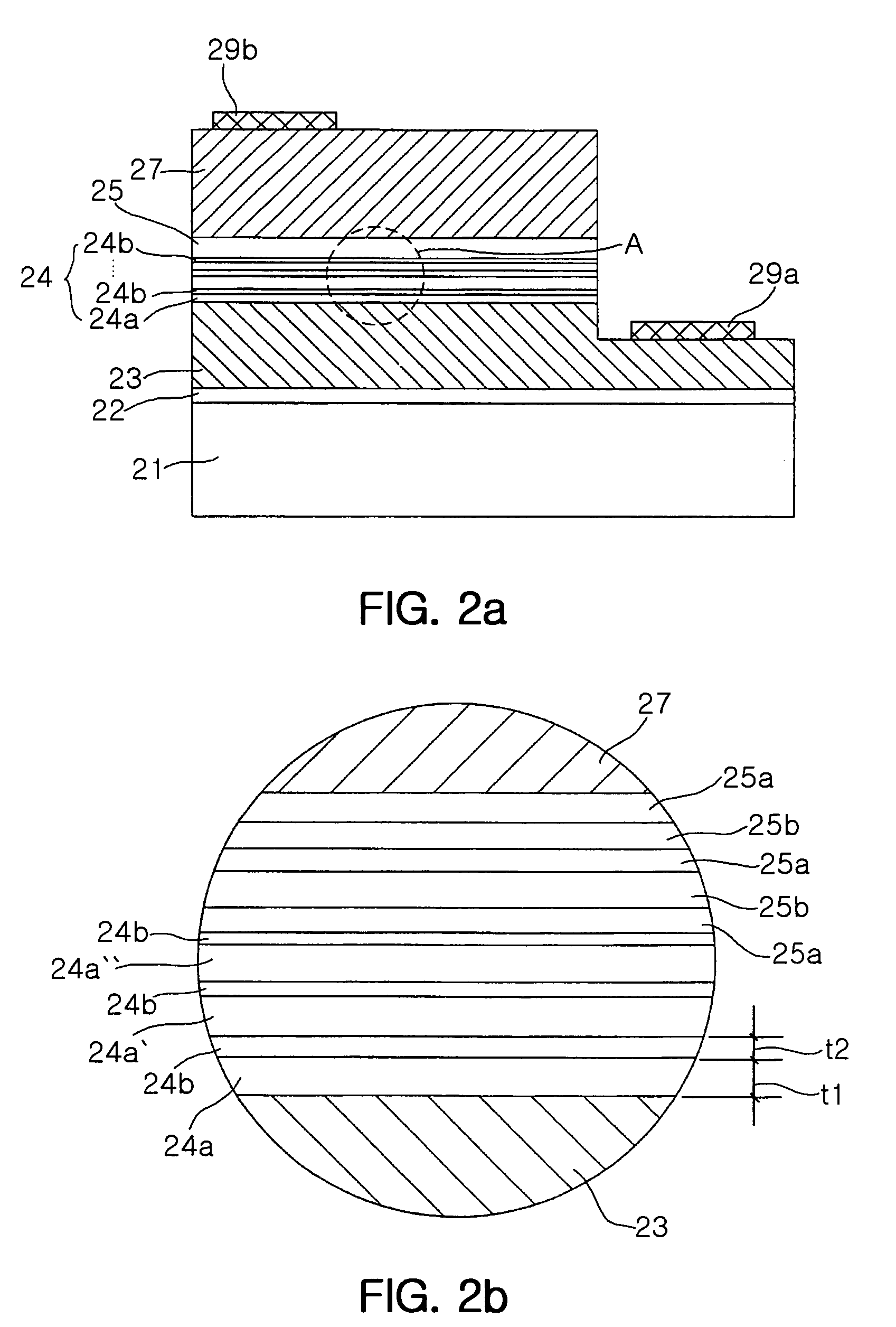
[0040]In order to confirm improvement effects of a nitride based semiconductor device in accordance with the present invention on the piezoelectric field, a nitride light emitting diode (LED) was prepared in a reactor under an atmosphere of ammonia (NH3) using trimethyl gallium (TMGa) and trimethyl Indium (TMIn) by MOCVD.

[0041]First, a GaN low temperature nucleus-growth layer was formed on a sapphire substrate, and then Si was used to form an n-type GaN layer having an impurity concentration of 4×10¹⁸ / cm3 and a thickness of 3 μm

[0042]Next, as presented in the present invention, a first nitride semiconductor layer satisfying a formula InyGa1-yN (0


PUM


Abstract

The present invention provides a nitride based semiconductor device comprising an active layer having a quantum well layer and a quantum barrier layer, wherein the device includes an electron emitting layer formed of at least two repeats of a first nitride semiconductor layer and a second nitride semiconductor layer having different compositions between a n-type nitride semiconductor layer and the active layer, the first nitride semiconductor layer has an energy band gap greater than that of the quantum well layer, smaller than that of the quantum barrier layer, and decreasing closer to the active layer, and the second nitride semiconductor layer has an energy band gap at least higher than that of the adjacent first nitride semiconductor layer(s) and has a thickness capable of tunneling electrons.

Description

RELATED APPLICATION[0001]The present application is based on, and claims priority from, Korean Application Number 2004-85789, filed on Oct. 26, 2004, the disclosure of which is incorporated by reference herein in its entirety.BACKGROUND OF THE INVENTION[0002]1. Field of the Invention[0003]The present invention relates to a nitride based semiconductor device, and more particularly to a high efficiency nitride based semiconductor device having improved internal quantum efficiency, operation voltage, and reverse voltage properties.[0004]2. Description of the Related Art[0005]Generally, nitride based semiconductor devices have been widely used in green light or blue light emitting diodes (LEDs) or laser diodes (LDs) provided as a light source for use in full color displays, image scanners, a variety of signaling systems and optical communication instruments. Such nitride based semiconductor devices include an active layer of a single quantum well (SQW) structure or a multi quantum well ...

Claims


Application Information

Patent Timeline
Patent Type & Authority Patents(United States)
IPC IPC(8): H01L29/06H01L31/072H01L33/06H01L33/32
CPCB82Y20/00H01L33/06H01L33/32H01S2304/12H01S5/3216H01S5/34333H01S5/0213
Inventor KIM, SUN WOONCHO, DONG HYUNKIM, JE WONLEE, KYU HANOH, JEONG TAKKIM, DONG JOON
Owner SAMSUNG ELECTRONICS CO LTD
Why Eureka
Try Eureka