Strained silicon CMOS on hybrid crystal orientations

a hybrid crystal orientation and silicon cmos technology, applied in the direction of transistors, semiconductor devices, electrical equipment, etc., can solve the problems of significant deformation of the electron mobility of (110) si surfaces, undesirable width of pfets, and inability to adapt to nfet devices, so as to achieve the effect of improving the performance of each type of devi

Inactive Publication Date: 2006-08-08
GLOBALFOUNDRIES INC
View PDF11 Cites 97 Cited by
  • Summary
  • Abstract
  • Description
  • Claims
  • Application Information

AI Technical Summary

Benefits of technology

[0009]One object of the present invention is to provide a method of integrating semiconductor devices such that different types of devices are formed upon a specific crystal orientation of a hybrid substrate that enhances the performance of each type of device.
[0011]A further object of the present invention is to improve the device performance of nFETs and further enhance the device performance of pFETs using a hybrid crystal orientated substrate that includes strained Si as an upper device layer in which nFETs and / or pFETs can be fabricated.

Problems solved by technology

To compensate for this discrepancy, pFETs are typically designed with larger widths in order to balance pull-up currents against the nFET pull-down currents and achieve uniform circuit switching. pFETs having larger widths are undesirable since they take up a significant amount of chip area.
Unfortunately, electron mobilities on (110) Si surfaces are significantly degraded compared to (100) Si surfaces.
As can be deduced from the above discussion, the (110) Si surface is optimal for pFET devices because of excellent hole mobility, yet such a crystal orientation is completely inappropriate for nFET devices.

Method used


Image

  • Strained silicon CMOS on hybrid crystal orientations
  • Strained silicon CMOS on hybrid crystal orientations
  • Strained silicon CMOS on hybrid crystal orientations

Examples


first embodiment

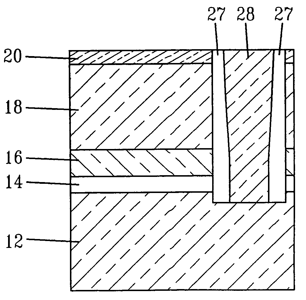
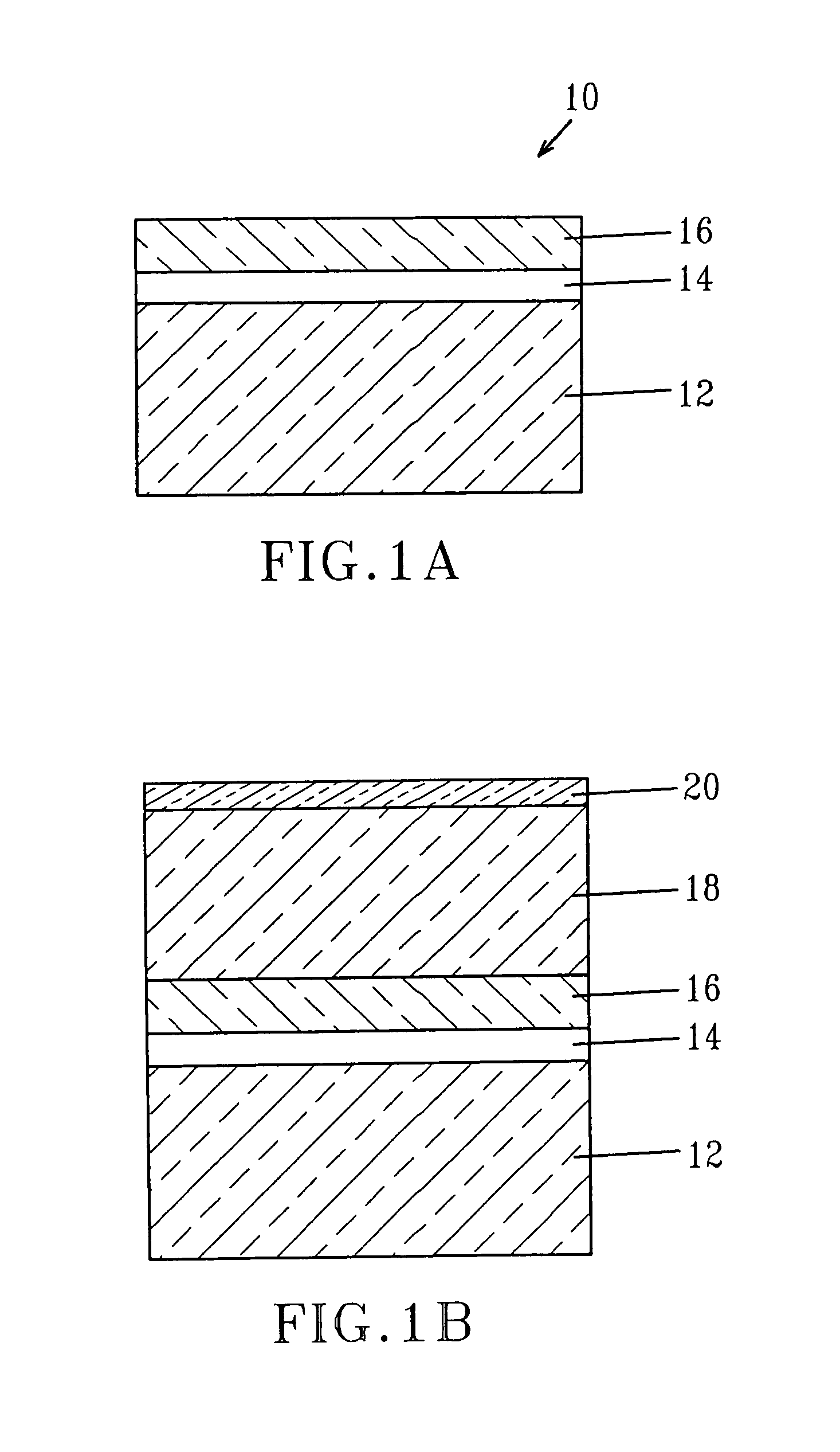
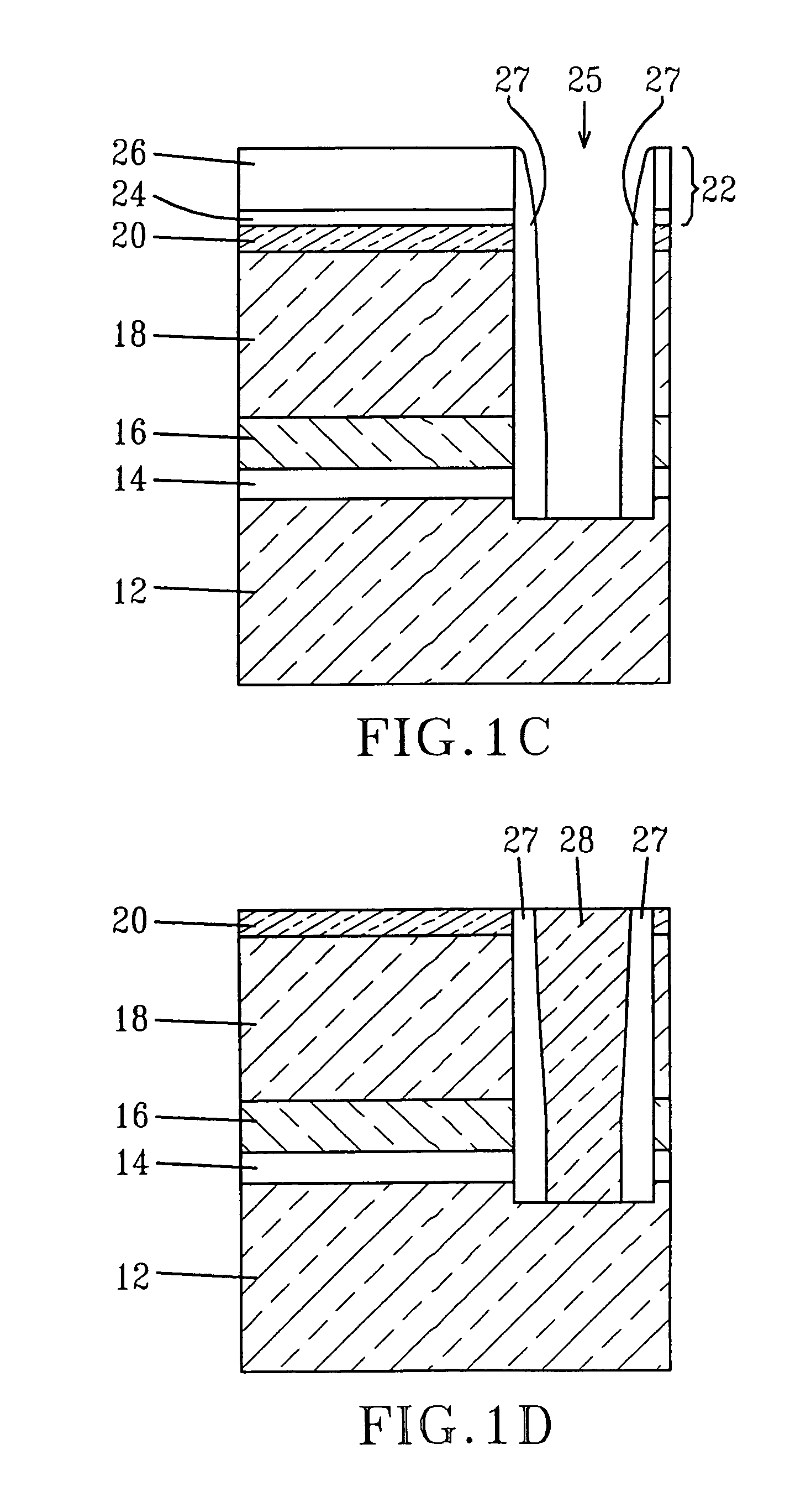
[0042]Referring to FIG. 1A, there is shown the hybrid substrate 10 that is employed in the present invention. The hybrid substrate 10 comprises a first semiconducting layer 12, a buried insulating layer 14 located on a surface of the first semiconducting layer 12, and a second semiconducting layer 14 located on a surface of the buried insulating layer 14. In accordance with the present invention, the first semiconducting layer 12 of the hybrid substrate 10 comprises a first semiconducting material that has a first crystallographic orientation and the second semiconducting layer 16 of the hybrid substrate 10 comprises a second semiconducting material that has a second crystallographic orientation which differs from the first crystallographic orientation.

[0043]The first semiconducting layer 12 of the hybrid substrate 10 is comprised of any semiconducting material including, for example, Si, SiC, SiGe, SiGeC, Ge, GaAs, InAs, InP as well as other III / V or II / VI compound semiconductors. ...

third embodiment

[0081]the present invention is slightly different from the first two embodiments mentioned above in that the process flow begins with first providing the structure shown in FIG. 3A which includes a first semiconducting layer 12 in the form of a relaxed SiGe alloy layer formed directly on a surface of a handle wafer 100. The handle wafer comprises any semiconducting or non-semiconducting substrate and the first semiconducting layer 12 is formed by a deposition process.

[0082]Next, the structure shown in FIG. 3A is bonded to a structure that includes a buried insulating layer 14 and a second semiconducting layer 16 so as to provide the structure shown in FIG. 3B.

[0083]A patterned hard mask layer 22 comprising oxide layer 24 and nitride layer 26 is then formed as described above and thereafter an opening that extends down to the relaxed SiGe alloy layer, i.e., first semiconducting layer 12, is formed through the patterned hard mask layer 22. A regrown semiconducting material 28 comprisi...

fifth embodiment

[0095]the present invention is shown in FIGS. 5A–E. Unlike the previous embodiments described above, the final strained Si-containing hybrid substrate shown in FIG. 5E has device regions that are both SOI like since buried insulating layers are present beneath the regrown semiconductor material 28 and the second semiconductor layer 16. FIG. 5A shows the initial structure of this embodiment of the present invention. Specifically, the initial structure shown in FIG. 5A includes a handle wafer 100, bottom insulating layer 102, first sacrificial semiconducting layer 12′ and SiGe alloy layer 50. The handle wafer 100 may include any semiconductor or non-semiconductor substrate well known in the art. Bottom insulating layer 102 is comprised of one of the insulators mentioned above in regard to buried insulating layer 14. The SiGe alloy layer 50 is formed as described above and that layer typically has a thickness of about 100 nm or less.

[0096]After providing the structure shown in FIG. 5A,...


PUM

PropertyMeasurementUnit
thicknessaaaaaaaaaa
thicknessaaaaaaaaaa
thicknessaaaaaaaaaa

Abstract

Methods of forming a strained Si-containing hybrid substrate are provided as well as the strained Si-containing hybrid substrate formed by the methods. In the methods of the present invention, a strained Si layer is formed overlying a regrown semiconductor material, a second semiconducting layer, or both. In accordance with the present invention, the strained Si layer has the same crystallographic orientation as either the regrown semiconductor layer or the second semiconducting layer. The methods provide a hybrid substrate in which at least one of the device layers includes strained Si.

Description

RELATED APPLICATIONS[0001]This application is related to co-pending and co-assigned U.S. patent application Ser. No. 10 / 250,241, filed Jun. 17, 2003, and co-pending and co-assigned U.S. patent application Ser. No. 10 / 696,634, filed Oct. 29, 2003, the entire contents of each of the aforementioned U.S. applications are incorporated herein by reference.FIELD OF THE INVENTION[0002]The present invention relates to high-performance metal oxide semiconductor field effect transistors (MOSFETs) for digital or analog applications, and more particularly to MOSFETs utilizing carrier mobility enhancement from surface orientation.BACKGROUND OF THE INVENTION[0003]In present semiconductor technology, CMOS devices, such as nFETs or pFETs, are typically fabricated upon semiconductor wafers, such as Si, that have a single crystal orientation. In particular, most of today's semiconductor devices are built upon Si having a (100) crystal orientation.[0004]Electrons are known to have a high mobility for a...

Claims


Application Information

Patent Timeline
Patent Type & Authority Patents(United States)
IPC IPC(8): H01L27/01H01L27/12H01L31/0392H01L27/08H01L21/02H01L21/20H01L21/336H01L21/762H01L21/8238H01L21/84H01L27/092H01L29/04H01L29/76H01L29/78H01L29/786
CPCH01L21/2022H01L21/76275H01L21/823807H01L27/1203H01L29/045H01L29/7842H01L21/84H01L29/78687
Inventor CHAN, KEVIN K.IEONG, MEIKEIREZNICEK, ALEXANDERSADANA, DEVENDRA K.SHI, LEATHENYANG, MIN
Owner GLOBALFOUNDRIES INC
Why Eureka
Try Eureka