
Integrated circuit design for signal integrity, avoiding well proximity effects

a technology of integrated circuits and signal integrity, applied in the direction of program control, total factory control, instruments, etc., can solve the problems of time-consuming and resource-intensive approaches, not desirable placement,

Inactive Publication Date: 2006-08-08
INT BUSINESS MASCH CORP
View PDF3 Cites 104 Cited by
  • Summary
  • Abstract
  • Description
  • Claims
  • Application Information

AI Technical Summary

Problems solved by technology

Depending on the expected sources of electrical noise and the required robustness of the IC design, it may or may not be desirable to place all transistors far enough away from a well edge to eliminate the effect.
Therefore, this approach is time consuming and resource intensive.

Method used


Image

  • Integrated circuit design for signal integrity, avoiding well proximity effects
  • Integrated circuit design for signal integrity, avoiding well proximity effects
  • Integrated circuit design for signal integrity, avoiding well proximity effects

Examples


Embodiment Construction

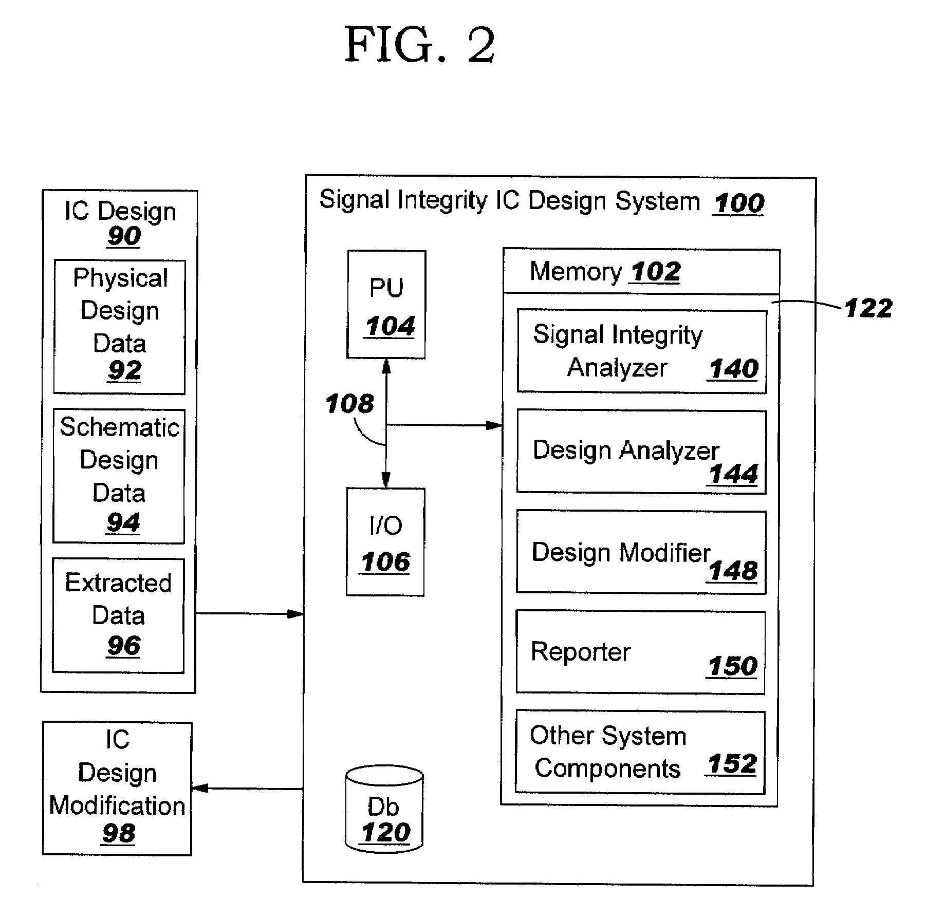
[0015]With reference to the accompanying drawings, FIG. 2 is a block diagram of a signal integrity IC design system 100 in accordance with the invention. Design system 100 includes a memory 102, a processing unit (PU) 104, input / output devices (I / O) 106 and a bus 108. A database 120 may also be provided for storage of data relative to processing tasks. It should be recognized that even though system 100 will be described in terms of a separate system, the teachings of the invention are equally applicable where system 100 is part of a larger IC design system (not shown).

[0016]Memory 102 includes a program product 122 that, when executed by PU 104, comprises various functional capabilities described in further detail below. Memory 102 (and database 120) may comprise any known type of data storage system and / or transmission media, including magnetic media, optical media, random access memory (RAM), read only memory (ROM), a data object, etc. Moreover, memory 102 (and database 120) may ...


PUM


Abstract

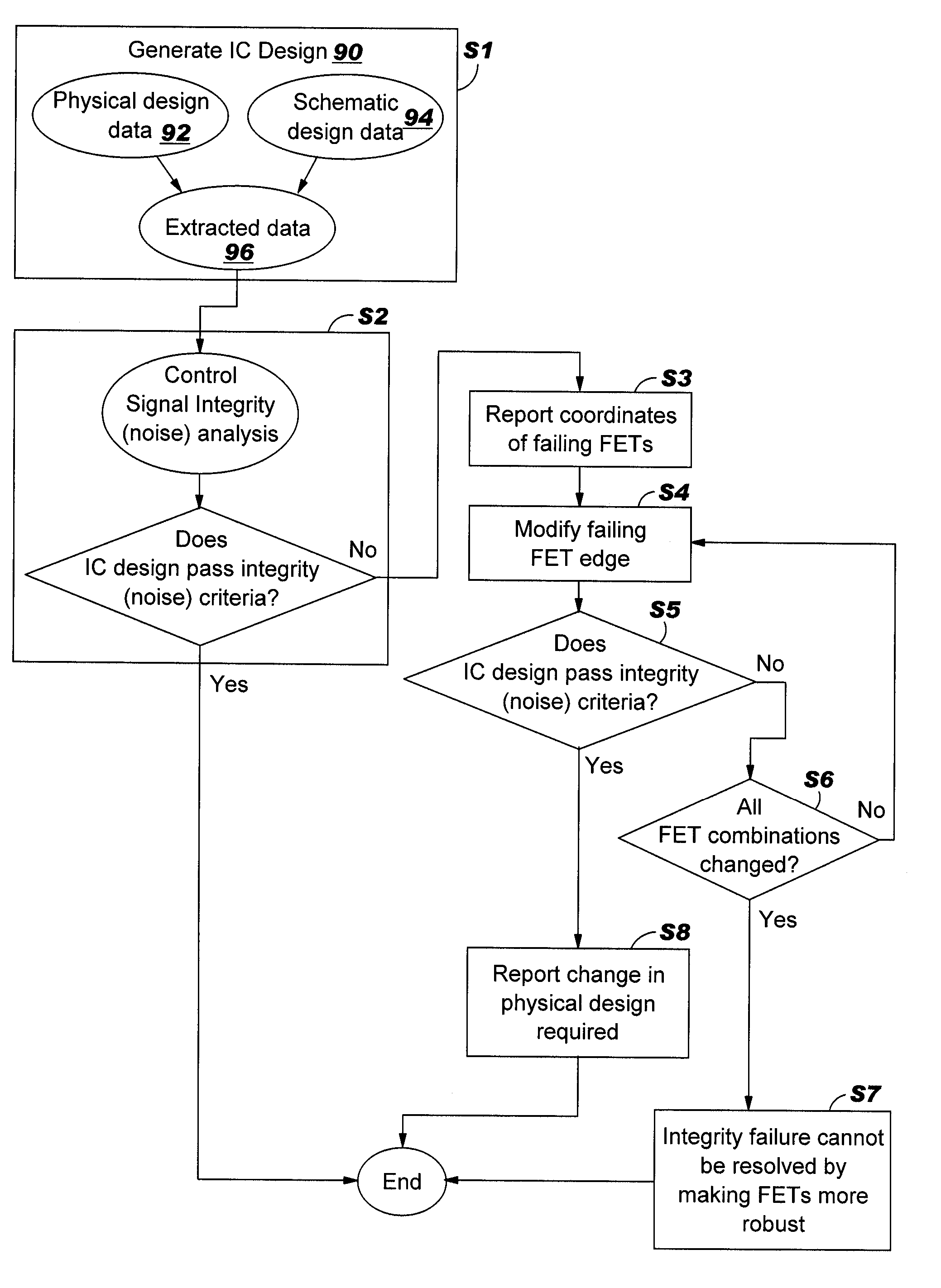
A method, system and program product for designing an integrated circuit (IC) for signal integrity. The invention conducts a signal integrity analysis on an IC design; identifies any field effect transistor (FET) that causes a signal integrity failure in the case that the IC design fails the signal integrity analysis; and modifies an edge of a failing FET that is closer than a threshold distance to a well edge. The invention eliminates the manual, iterative procedure for determining the device causing a signal integrity failure due to well proximity effects.

Description

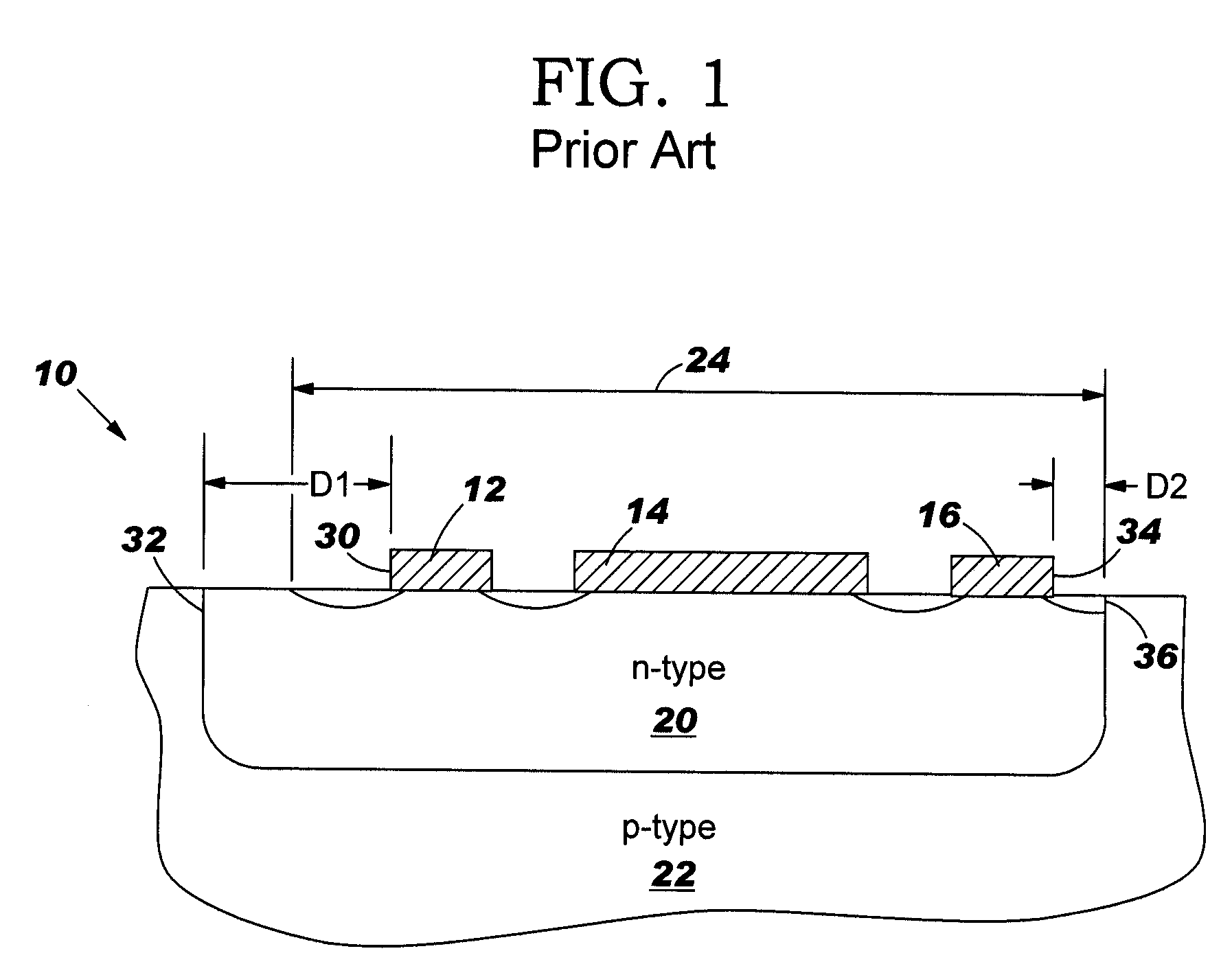
BACKGROUND OF INVENTION[0001]1. Technical Field[0002]The present invention relates generally to integrated circuit design, and more particularly, relates to a system, method and program product for designing an IC for signal integrity due to well proximity effects.[0003]2. Related Art[0004]In very large scale integrated (VLSI) circuit design, the proximity of a transistor's source or drain diffusion to a well edge affects its threshold voltage. Transistors designed in the same technology, even on the same integrated circuit (IC), will have different threshold voltages (Vt) depending on their active area's proximity to an implanted well edge. For example, FIG. 1 illustrates conventional complementary metal oxide semiconductor (CMOS) p-type field effect transistors (FET) 10 including a first device 12, a second device 14 and a third device 16. Devices 12, 14, 16 are located over an n-type well 20 that is positioned within a p-type substrate 22. An area 24 is considered an active area....

Claims


Application Information

Patent Timeline
Patent Type & Authority Patents(United States)
IPC IPC(8): G06F17/50G06F9/45H01L27/02
CPCG06F17/5081H01L27/0207G06F2217/12G06F30/398G06F2119/18Y02P90/02
Inventor BARD, KAREN A.ROSE, RONALD D.SITKO, MICHAEL H.
Owner INT BUSINESS MASCH CORP
Learn More