Semiconductor device and method of manufacturing the same

a semiconductor and semiconductor technology, applied in the direction of semiconductor devices, electrical devices, transistors, etc., can solve the problems of large diffusion coefficient of impurities in silicon, low resistance, and difficult to obtain a shallow impurity diffusion layer , to achieve the effect of forming a shallow impurity diffusion layer having a junction of about 20 nm or less, and achieving the effect of small diffusion coefficien

Inactive Publication Date: 2006-08-15
KK TOSHIBA
View PDF15 Cites 36 Cited by
  • Summary
  • Abstract
  • Description
  • Claims
  • Application Information

AI Technical Summary

Benefits of technology

[0011]A first aspect of the present invention is a method for manufacturing a semiconductor device comprising: implanting ions of an impurity element into a semiconductor region; implanting, into the semiconductor region, ions of a predetermined element which is a group IV element or an element having the same conductivity type as the impurity element and larger in mass number than the impurity element; and irradiating a region into which the impurity element and the predetermined element are implanted with light to anneal the region, the light having an emission intensity distribution, a maximum point of the distribution existing in a wavelength region of not more than 600 nm.

Problems solved by technology

However, these impurities have larger diffusion coefficients in silicon (Si).
This gradually makes it difficult to obtain a shallow impurity diffusion layer.
By RTA using a halogen lamp, therefore, it is difficult to form an impurity diffusion layer having a shallow (about 20 nm or less) junction and low resistance.
Unfortunately, the light of the flash lamp is reflected by the surface of a semiconductor substrate to worsen the heating efficiency.
This makes sufficient impurity activation difficult.
If the irradiation energy of the flash lamp is increased to raise the activation ratio, the thermal stress increases, and this destroys the semiconductor substrate.
That is, the conventional flash lamp annealing method can form an impurity diffusion region having a shallow junction but cannot unlimitedly lower the resistance of the diffusion layer.
Since, however, the light-absorbing film formed on the surface of a gate insulating film is used, efficient heating is difficult to perform.
However, the use of the light-absorbing film formed on the surface of an interlayer insulating film also makes efficient heating difficult.
However, accurately controlling the impurity profile is conventionally difficult.

Method used


Image

  • Semiconductor device and method of manufacturing the same
  • Semiconductor device and method of manufacturing the same
  • Semiconductor device and method of manufacturing the same

Examples


first embodiment

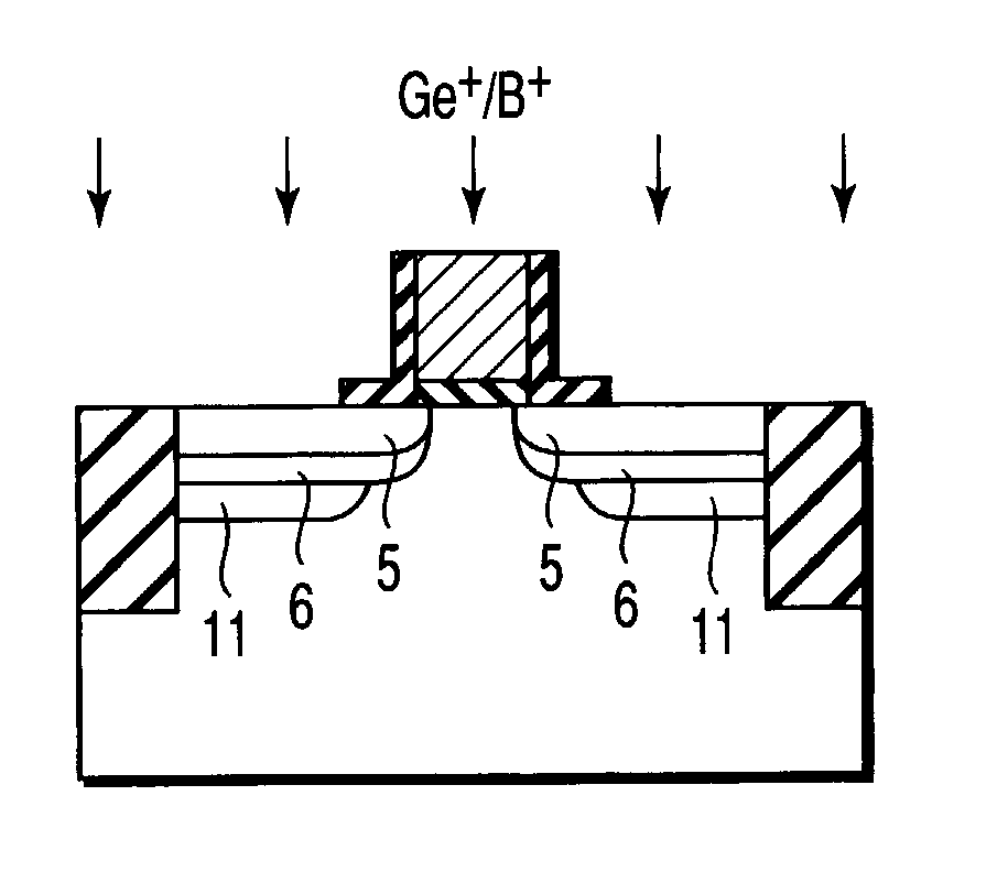
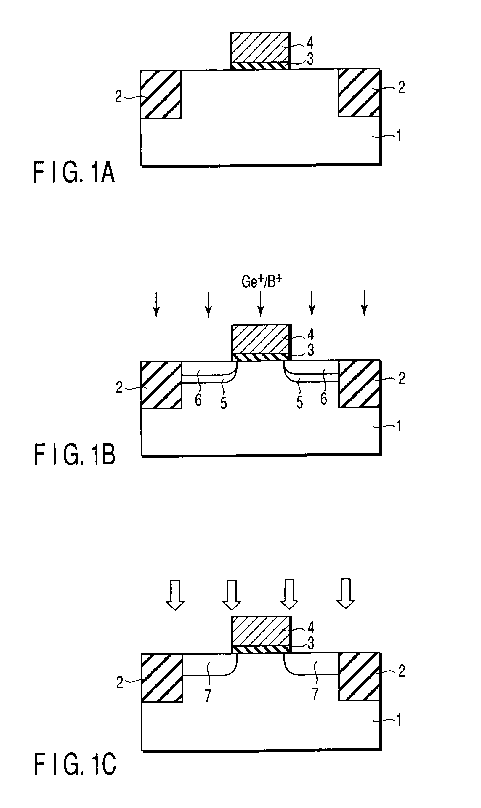
[0032]FIGS. 1A to 1C are sectional views showing a semiconductor device fabrication method according to the first embodiment of the present invention. This method will be explained by taking the fabrication steps of a p-type MOS transistor as an example.

[0033]First, as shown in FIG. 1A, in accordance with the conventional p-type MOS transistor fabrication method, isolation regions 2 are formed in an n-type silicon (Si) substrate 1. After that, a gate insulating film (silicon oxide film) 3 is formed, and a gate electrode 4 is formed on this gate insulating film 3.

[0034]Next, as shown in FIG. 1B, the gate electrode 4 is used as a mask to implant germanium (Ge) ions into the surface region of the n-type silicon substrate 1. The conditions of this ion implantation are an acceleration energy of 15 keV and a dose of 5×1014 cm−2. By this ion implantation, crystal defect regions 5 are formed in the surface of the silicon substrate 1. For example, amorphous crystal defect regions 5 are forme...

second embodiment

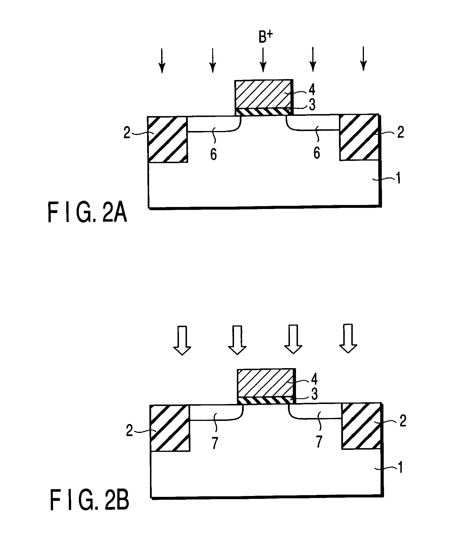
[0052]FIGS. 10A to 10C are sectional views showing a semiconductor device fabrication method according to the second embodiment of the present invention. This method will be explained by taking the fabrication steps of a p-type MOS transistor as an example.

[0053]In this embodiment, an ion implantation region (Ge diffusion layer) of Ge (predetermined element) is shallower than an ion implantation region (B diffusion layer) of B (impurity element). More specifically, the density of Ge is made lower than that of B at the boundary (p-n junction boundary) between an n-type semiconductor substrate and a p-type B diffusion layer. From another viewpoint, a position at which the Ge density is equal to the B density at the p-n junction boundary is present between the surface of a semiconductor substrate and the p-n junction boundary. For example, the B density at the p-n junction boundary is about 1×10¹⁸ / cm3. From still another viewpoint, a position at which the density distribution of Ge is ...

third embodiment

[0069]FIGS. 12A to 12C are sectional views showing a semiconductor device fabrication method according to the third embodiment of the present invention. This method will be explained by taking the fabrication steps of a p-type MOS transistor as an example.

[0070]In this embodiment, Ga is used instead of Ge as an element for forming crystal defect regions 5. Additionally, an ion implantation region (Ga diffusion layer) of Ga (predetermined element) is shallower than an ion implantation region (B diffusion layer) of B (impurity element).

[0071]First, as shown in FIG. 12A, in accordance with the conventional p-type MOS transistor fabrication method, isolation regions 2 are formed in an n-type silicon (Si) substrate 1. After that, a gate insulating film (silicon oxide film) 3 is formed, and a gate electrode 4 is formed on this gate insulating film 3.

[0072]Next, as shown in FIG. 12B, the gate electrode 4 is used as a mask to ion-implant Ga into the surface region of the n-type silicon subs...


PUM


Abstract

Disclosed is a method for manufacturing a semiconductor device comprising implanting ions of an impurity element into a semiconductor region, implanting, into the semiconductor region, ions of a predetermined element which is a group IV element or an element having the same conductivity type as the impurity element and larger in mass number than the impurity element, and irradiating a region into which the impurity element and the predetermined element are implanted with light to anneal the region, the light having an emission intensity distribution, a maximum point of the distribution existing in a wavelength region of not more than 600 nm.

Description

CROSS-REFERENCE TO RELATED APPLICATIONS[0001]This application is based upon and claims the benefit of priority from the prior Japanese Patent Application No. 2002-113570, filed Apr. 16, 2002, the entire contents of which are incorporated herein by reference.BACKGROUND OF THE INVENTION[0002]1. Field of the Invention[0003]The present invention relates to a semiconductor device and a semiconductor device manufacturing method and, more particularly, to a thermal annealing technology.[0004]2. Description of the Related Art[0005]High integration of LSIs has been achieved by reducing sizes of elements constructing LSIs. With decreasing dimensions of elements, the formation of a shallow p-n junction, i.e., the formation of a shallow impurity diffusion region is becoming important.[0006]To form this shallow impurity diffusion region, ion implantation at low acceleration energy and optimization of subsequent annealing are important. Boron (B) is used as a p-type impurity, and phosphorus (P) a...

Claims


Application Information

Patent Timeline
Patent Type & Authority Patents(United States)
IPC IPC(8): H01L21/425H01L21/265H01L21/268H01L21/336H01L29/78
CPCH01L21/26506H01L21/26513H01L29/6659H01L29/6653H01L21/2686H01L29/66575H01L21/324
Inventor ITO, TAKAYUKIIINUMA, TOSHIHIKOSUGURO, KYOICHI
Owner KK TOSHIBA
Why Eureka
Try Eureka