Forming method and a forming apparatus of nanocrystalline silicon structure

a forming method and nanocrystalline silicon technology, applied in the field of forming methods and forming apparatus of nanocrystalline silicon structure with oxide or nitride, can solve the problems of insufficient nanoscale silicon crystal grains packing density, inability to meet the requirements of wet process anodic oxidation, and low packing density of nanoscale silicon crystal grains, so as to improve the uniformity of substrate surface treatment and termination treatment, improve the effect of crystal structure perfection

Inactive Publication Date: 2006-08-15
ANELVA CORP +1
View PDF3 Cites 15 Cited by
  • Summary
  • Abstract
  • Description
  • Claims
  • Application Information

AI Technical Summary

Benefits of technology

[0009]For the application of the nanocrystalline silicon structure to various devices, it is required that the size of crystal grains can be highly controlled at the nanometer level, and the nanoscale silicon crystal grains are packed with high density and stably terminated. In addition, the nanocrystalline silicon structure is preferably prepared by a low-temperature process (lower than 600° C.) so that a glass substrate can be used, and the preparation cost is desired to be low, which is an important condition for the forming method of nanocrystalline silicon structure. In the case of an LSI application, it is preferable that the forming method of nanocrystalline silicon structure is comprised of dry processes only.

Problems solved by technology

However, a wet process of the anodic oxidation is inevitable in this method.
Furthermore, since the anodic oxidation is employed to etch silicon and prepare the structure, the packing density of the nanoscale silicon crystal grains is not sufficient.
However, the packing density of nanoscale silicon crystal grains is very low even when compared to that prepared by using the anodic oxidation method.
Moreover, in order to precipitate nanoscale silicon single crystal grains, the annealing process must be carried out at a high temperature around 1000° C., which makes it impossible to employ a glass substrate.

Method used


Image

  • Forming method and a forming apparatus of nanocrystalline silicon structure
  • Forming method and a forming apparatus of nanocrystalline silicon structure
  • Forming method and a forming apparatus of nanocrystalline silicon structure

Examples


Embodiment Construction

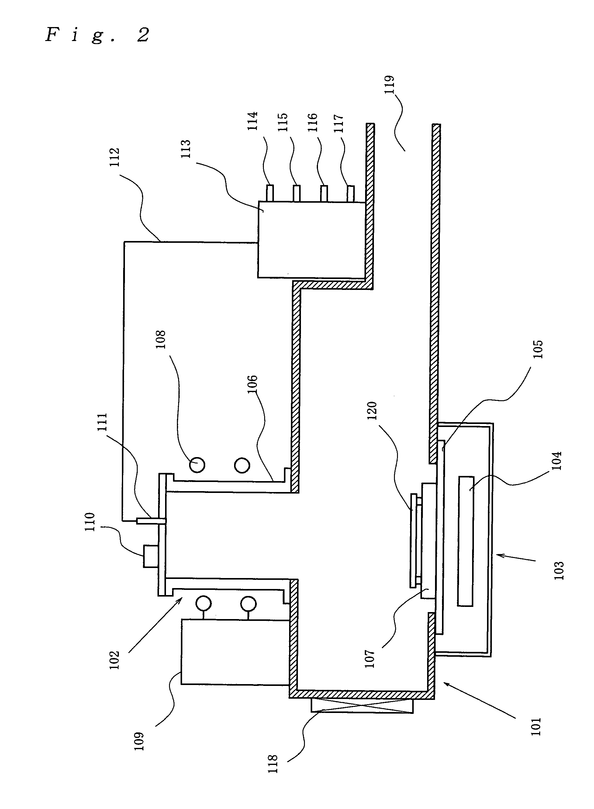
[0027]An embodiment of this invention is explained by referring to the drawings.

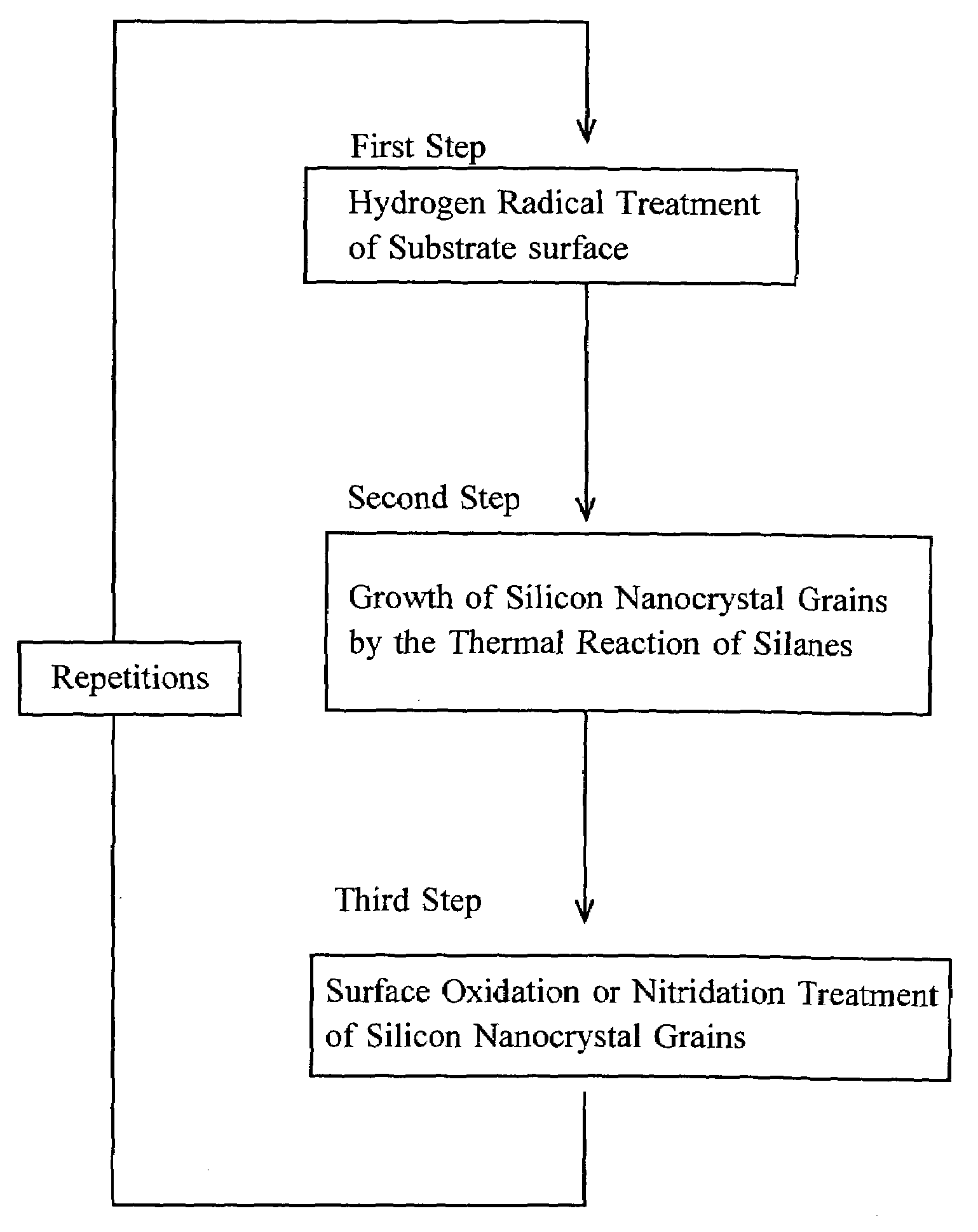
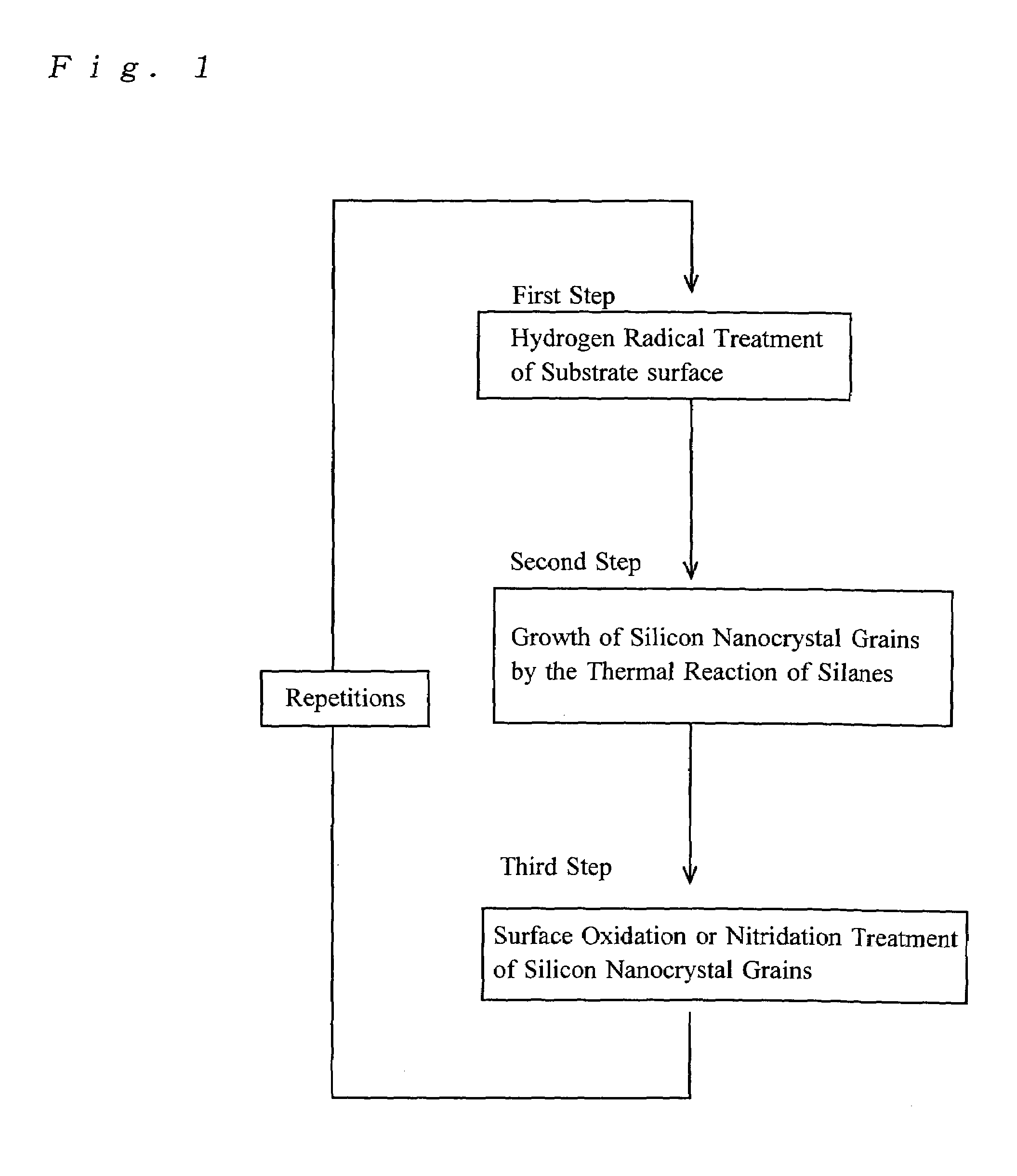
[0028]FIG. 1 is a flow chart explaining an embodiment of the present invention. In a forming method of nanocrystalline silicon structure of this invention, as is shown in FIG. 1, according to a first step, a surface of a substrate is treated with hydrogen radicals; in a second step, silicon nanocrystal grains are deposited on the substrate by the thermal reaction of a silicon-containing gas; and in a third step in, the surfaces of the silicon nanocrystal grains are terminated with oxygen or nitrogen using an oxygen gas, an oxygen radical or a nitrogen radical. The three steps are repeated until the nanocrystalline silicon structure comes to a predetermined thickness.

[0029]That is, in the hydrogen radical treatment, the nucleation sites for silicon nanocrystal grain growth are formed over the whole surface of the substrate. For example, in the case of a silicon substrate, a natural oxide film is generally...


PUM

PropertyMeasurementUnit
grain sizeaaaaaaaaaa
diameteraaaaaaaaaa
thicknessaaaaaaaaaa

Abstract

A forming method and a forming apparatus of nanocrystalline silicon structure makes it possible to prepare a nanocrystalline silicon structure at a low temperature to have densely packed silicon crystal grains which are stably terminated and to effectively control the grain size in nanometer scale. A forming method and a forming apparatus of nanocrystalline silicon structure with oxide or nitride termination, carry out a first step of treating a surface of a substrate with hydrogen radical; a second step of depositing silicon crystals having a grain size of 10 nm or less by the thermal reaction of a silicon-containing gas; and a third step of terminating the surface of the silicon crystal with oxygen or nitrogen by using one of oxygen gas, oxygen radical and nitrogen radical.

Description

CROSS-REFERENCE TO RELATED APPLICATIONS[0001]The present application claims the priority of JP 2003-307592, filed in Japan on Aug. 29, 2003, the entire contents of which are incorporated herein by reference.BACKGROUND OF THE INVENTION[0002]1. Field of the Invention[0003]The present invention relates to a forming method and a forming apparatus of nanocrystalline silicon structure with oxide or nitride termination, and more particularly to a forming method and forming apparatus of nanocrystalline silicon structure carried out by using dry processes only.[0004]2. Description of Related Art[0005]A nanocrystalline silicon structure with oxide or nitride termination is composed of a large number of silicon single crystals which have a grain size of 10 nm or less and are terminated with oxygen or nitrogen. Since the nanocrystalline silicon structure shows unique physical phenomena as to electron confinement, photoluminescence and electron emission, it has been noticed for its possibility o...

Claims


Application Information

Patent Timeline
Patent Type & Authority Patents(United States)
IPC IPC(8): H01L21/31B82B3/00C01B33/02C23C16/02C23C16/24C23C16/56H01L21/00H01L21/205H01L21/316H01L21/318H01L21/322H01L29/06
CPCB82Y30/00C23C16/02C23C16/24C23C16/56H01J37/321H01L21/02661H01L21/0237H01L21/02381H01L21/02532H01L21/0262H01J2237/2001H01L21/3185H01L21/31662H01L21/32105H01L21/02664
Inventor NUMASAWA, YOICHIROKOSHIDA, NOBUYOSHI
Owner ANELVA CORP
Why Eureka
Try Eureka