
Method for tuning a digital design for synthesized random logic circuit macros in a continuous design space with optional insertion of multiple threshold voltage devices

a random logic and design space technology, applied in computer aided design, program control, instruments, etc., to achieve the effect of minimizing “binning errors, optimizing more effective, and efficient and effective methods

Inactive Publication Date: 2006-08-15
GLOBALFOUNDRIES INC
View PDF16 Cites 234 Cited by
  • Summary
  • Abstract
  • Description
  • Claims
  • Application Information

AI Technical Summary

Benefits of technology

[0029]Disclosed is an efficient and effective methodology for obtaining timing closure in the design of large, complex, high-performance digital integrated circuits. The novel methodology includes the use of a tuner on random logic macros that adjusts transistor sizes in a continuous domain. To accommodate this tuning, logic gates are mapped to parameterized cells for the tuning process and then back to fixed gates after tuning. Tuning is constrained in such a way as to minimize “binning errors” when the design is mapped back to fixed cells. Further, the critical sections of the circuit are marked in order to make the optimization more effective and to fit within the problem-size constraints of the tuner. A specially formulated objective function is employed during the tuning to promote faster global timing convergence, despite possibly incorrect initial timing budgets. The specially formulated objective function targets all paths that are failing timing, with appropriate weighting, rather than just targeting the most critical path. Finally, the addition of multiple threshold voltage gates allows for increased performance while limiting leakage power.

Problems solved by technology

It is widely known that efficient implementations of such macros cannot be totally developed by automatic computer-aided design (CAD) software and that in-depth engineering is required in many steps to assure performance.
Typically the optimal cycle time for a given technology is not achieved due to the imperfections within this system including approximations made along the way and short cuts taken throughout the process to achieve a quick turnaround from the design system.
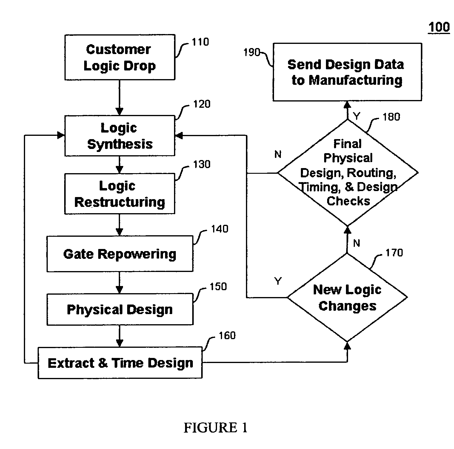
A flat design flow as in FIG. 1 (flow 100) implies very large optimization problems with very large design spaces.
The use of heuristic methods leads to a number of difficulties including problems in achieving performance, a large number of design iterations, incomplete exploitation of the technology, all of which lead to long design times and sub-optimal designs.
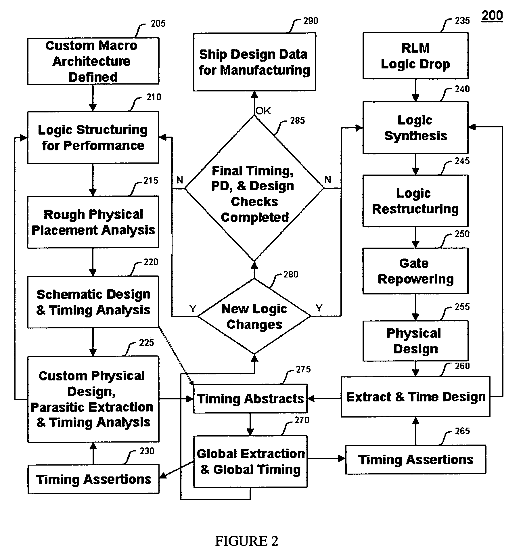
Referring back to FIG. 2 (flow 200), the difficulty with this flow is the management of the timing budgets between macros and global connections.
Another potential problem is that typically only the top most critical path or paths are searched, broken down and analyzed for the required solution, but as soon as that is done, other sub-critical paths which were not exposed before may now be limiting.
The procedure is therefore time-consuming and not guaranteed to produce a design that meets the required system-level performance.
Thus, the hierarchical design flow of FIG. 2 (flow 200) suffers from two main problems.
The first is the difficulty of iteratively adjusting the budgets of the individual macros so as to meet global timing requirements, while giving individual macros reachable targets.
The second is that focusing on just a few critical paths is not sufficient to meet overall timing and leads to a great deal of re-design.
As described in the previous two paragraphs, both flows limit the progression of the design due to the nature of the heuristic iterations that each flow applies and therefore retards the achievable circuit performance which can be obtained by the flows.
This slow convergence rate towards cycle time objectives limits the flexibility of the design team to introduce functional and timing changes throughout the design process, and in particular during the crucial period late in the design cycle.
Low threshold voltage (Low Vt) transistors offer faster performance, but at the cost of increased leakage power.
High threshold voltage (High Vt) transistors offer significant reduction in leakage power, but at the cost of lower performance.
It is therefore beneficial to sparingly use Low Vt devices on the critical paths to achieve higher performance, but limit the usage of such devices to limit leakage power.
The prior-art heuristic methods limit the ability to optimally adjust the performance and leakage of the circuits.
The prior art therefore suffers from several problems and weaknesses as summarized below:a) Prior art design flows generally require excessive iteration.b) Prior art design flows focus on optimizing only the single or a very small subset of the most critical paths, which in turn leads to long design times and slow convergence towards cycle time objectives.c) In prior art hierarchical flows, the interaction between imperfect budgeting across the hierarchy at the global level and imperfect optimization at the macro level can lead to poor circuit performance and excessive redesign effort.d) Prior art flows do not include continuous optimization techniques during RLM design, despite the ability of such techniques to obtain optimal solutions.
Further, prior-art flows do not include specialized techniques to deal with the relatively low capacity and high run times of such continuous optimization methods.

Method used


Image

  • Method for tuning a digital design for synthesized random logic circuit macros in a continuous design space with optional insertion of multiple threshold voltage devices
  • Method for tuning a digital design for synthesized random logic circuit macros in a continuous design space with optional insertion of multiple threshold voltage devices
  • Method for tuning a digital design for synthesized random logic circuit macros in a continuous design space with optional insertion of multiple threshold voltage devices

Examples


Embodiment Construction

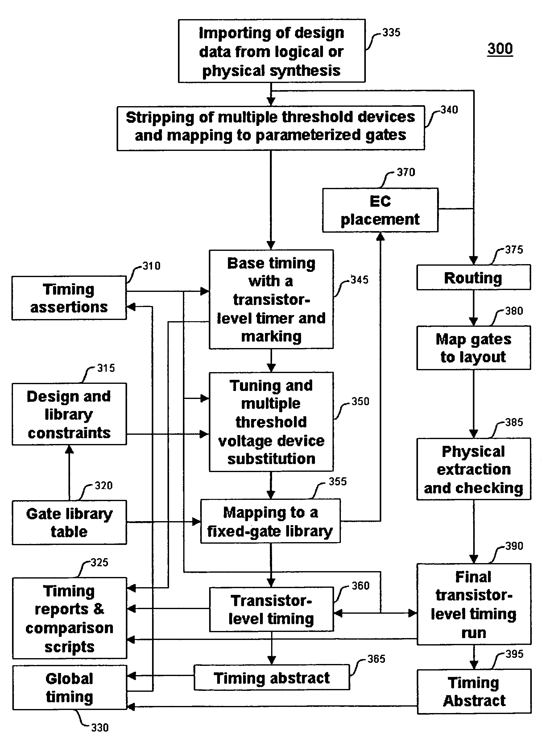
[0038]An inventive design and optimization methodology for random logic macros (RLMs) is shown in FIG. 3 (flow 300). The salient features of the preferred components of this methodology and how they fit together are explained below.

[0039]Referring to FIG. 3, the first step is to import design data (box 335) that comes out of a logical or physical synthesis program, which is known to be logically correct. This design data is at the gate-level, i.e., it typically consists of a collection of logic gate primitives such as NAND gates, NOR gates, etc. These primitives are called “fixed cells” since they are available in fixed transistor size combinations in the library of logic gates. As will be described in detail below, the inventive methodology maps the fixed-cell gate-level design to an equivalent “parameterized cell” transistor-level design in order to apply sophisticated mathematical optimization techniques, and then finally returns the design to a fixed-cell gate-level description....


PUM


Abstract

A Digital Design Method which may be automated is for obtaining timing closure in the design of large, complex, high-performance digital integrated circuits. The methodincludes the use of a tuner on random logic macros that adjusts transistor sizes in a continuous domain. To accommodate this tuning, logic gates are mapped to parameterized cells for the tuning and then back to fixed gates after the tuning. Tuning is constrained in such a way as to minimize “binning errors” when the design is mapped back to fixed cells. Further, the critical sections of the circuit are marked in order to make the optimization more effective and to fit within the problem-size constraints of the tuner. A specially formulated objective function is employed during the tuning to promote faster global timing convergence, despite possibly incorrect initial timing budgets. The specially formulated objective function targets all paths that are failing timing, with appropriate weighting, rather than just targeting the most critical path. Finally, the addition of multiple threshold voltage gates allows for increased performance while limiting leakage power.

Description

CROSS-REFERENCE TO RELATED APPLICATIONS[0001]This application is a continuation in part of these referenced patent applications and contains subject matter which is related to the subject matter of the following co-pending applications, each of which is assigned to the same assignee as this application, International Business Machines Corporation of Armonk, N.Y.. Each of the two patent applications from which priority is claimed are listed below and hereby incorporated herein by reference in its entirety:[0002]D. J. Hathaway, L. K. Lange, C. Visweswariah and P. M. Williams, “Method of Optimizing and Analyzing Selected Portions of a Digital Integrated Circuit,” U.S. patent application Ser. No. 10 / 436,213, filed on May 12, 2003, assigned to IBM, and issued Mar. 7, 2006 as U.S. Pat. No. 7,010,763.[0003]D. J. Hathaway, C. Visweswariah, P. M. Williams, J. Zhou, “Method of Achieving Timing Closure in Digital Integrated Circuits by Optimizing individual Macros,” U.S. Pat. application Ser. ...

Claims


Application Information

Patent Timeline
IPC IPC(8): G06F17/50
CPCG06F17/505G06F30/327
Inventor WILLIAMS, PATRICK M.CHO, EE K.HATHAWAY, DAVID J.HSU, MEI-TINGLANGE, LAWRENCE K.NORTHROP, GREGORY A.VISWESWARIAH, CHANDRAMOULIWASHBURN, CINDY SHUIKINGZHOU, JUN
Owner GLOBALFOUNDRIES INC
Learn More