Piezoelectric resonator and method for manufacturing the same

a technology of piezoelectric resonators and resonators, which is applied in piezoelectric/electrostrictive/magnetostrictive devices, piezoelectric/electrostrictive/magnetostriction machines, and details of piezoelectric/electrostrictive devices. it can solve the problem of insufficient etching that does not completely interconnect the small rectangular holes, and the product is sharply reduced. the effect of reliability

Active Publication Date: 2006-08-29
SEIKO EPSON CORP
View PDF8 Cites 38 Cited by
  • Summary
  • Abstract
  • Description
  • Claims
  • Application Information

AI Technical Summary

Benefits of technology

[0079]According to the present invention, the marginal edges of the openings of the both masks (in particular, the marginal edges in the crystal orientation in which the etching rate is low) are predisplaced as predetermined to bring the marginal

Problems solved by technology

Accordingly, in the case of cutting the wafer along the dicing grooves 131 by means of a dicing blade or similar cutting means, cracking readily occurs in the annular marginal portion 104 and the resonating portion 103, giving rise to a problem of sharp reduction in productivity.
This constitutes an obstacle to a reduction in profile of the package and ignores the demand for miniaturization.
However, the diameter (width) of each through hole 140H to be formed within the width of the connecting pad 112b on the ultraminiature crystal resonating element measuring, for instance, less than 1.3×0.9 mm inevitably becomes as small as on the order of μ—this causes frequent occurrence of insufficient etching that does not completely interconnect the small rectangular holes made in each crystal substrate from its top and underside surfaces.
It is particularly difficult to form two through holes in one marginal edge face of each piezoelectric substrate of an extremely small area.
In the formation of concavities by chemical etching in individual piezoelectric substrate regions on a sheet-like piezoelectric substrate wafer with a plurality of piezoelectric substrates arranged in a matrix form, it is difficult to make uniform the thicknesses of all ultrathin resonating portions formed by concavity bottom portions.
Moreover, there is a fear that the surface tension of the etchant 155 filling the concavity 102 prevents it from making full contact with the entire area of the bottom of the concavity, leaving therein unetched portions 156 as shown in FIG. 18(d), and hence resulting in the individual etching becoming unsuccessful.
As described above, in the case of individual etching of the concavities to remove variations in the depths of the concav

Method used


Image

  • Piezoelectric resonator and method for manufacturing the same
  • Piezoelectric resonator and method for manufacturing the same
  • Piezoelectric resonator and method for manufacturing the same

Examples


Embodiment Construction

[0116]The present invention will hereinafter be described in detail with reference to its embodiments shown in the drawings.

Embodiment Corresponding to First Prior Art Example

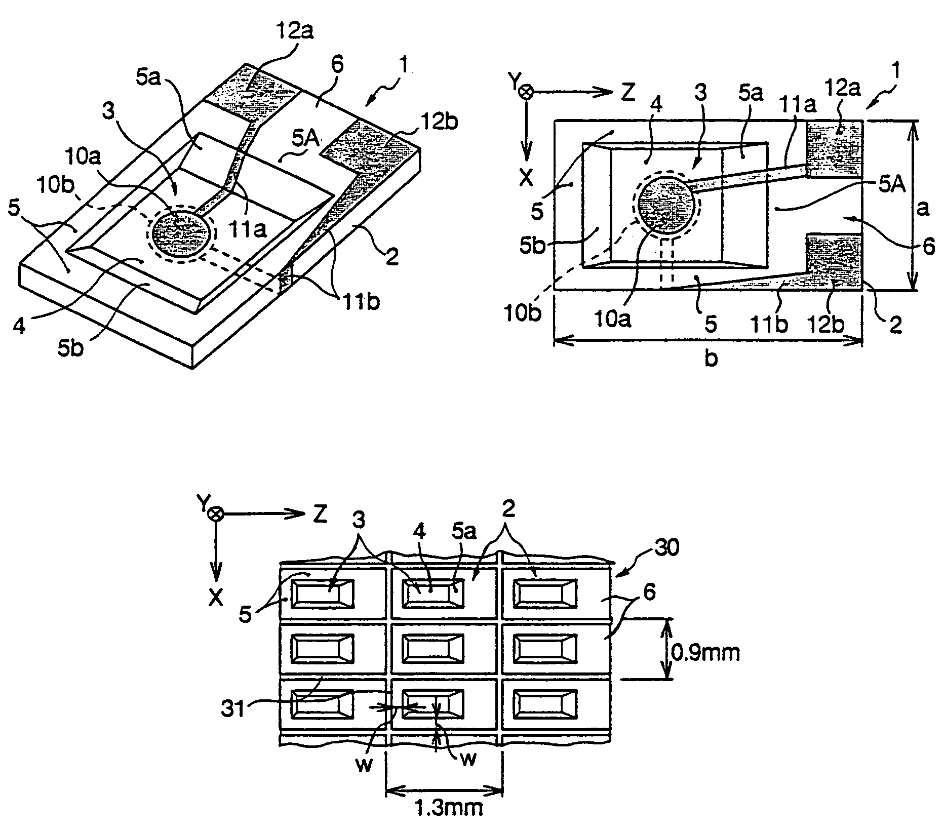
[0117]FIGS. 1(a) and (b) are perspective view and plan views showing a crystal resonating element 1 made of an AT-cut crystal as an example of the piezoelectric resonating element according to an embodiment of the present invention.

[0118]The crystal resonating element 1 is provided with a crystal substrate 2 made of an AT-cut crystal as an anisotropic piezoelectric material, excitation electrodes formed on both major surfaces of the crystal substrate 2, respectively, lead electrodes 11a and 11b extending from the excitation electrodes 10a and 10b, respectively, and connecting pads 12a and 12b forming respective lead electrode end portions.

[0119]The crystal substrate 2 has a construction in which an ultrathin resonating portion 4 is formed by the bottom of a concavity 3 formed by etching in one of major surfaces...


PUM


Abstract

In the case where an ultraminiature piezoelectric substrate, which has a resonating portion formed by making a concavity by etching in the surface of the piezoelectric substrate made of an anisotropic crystal material, is mass-produced by batch operation using a large-area piezoelectric substrate wafer, an annular portion surrounding each concavity is formed sufficiently thick to prevent cracking from occurring when the wafer is severed. A piezoelectric substrate 2 of an anisotropic piezoelectric crystal material has a thin resonating portion 4 and a thick annular portion 5 integrally surrounding the outer marginal edge of the resonating portion to form a concavity 3 in at least one of major surfaces of the substrate; the inner wall 5a of the annular portion in the one crystal orientation slopes gently more than the inner wall in the other crystal orientation perpendicular to said one crystal orientation, and the piezoelectric substrate is longer in said one crystal orientation than in the other crystal orientation.

Description

BACKGROUND OF THE INVENTION[0001]1. Field of the Invention[0002]The present invention relates to improvements in a piezoelectric substrate of a structure having an ultra-thin resonating portion surrounded with a thick annular marginal portion formed integrally therewith, a piezoelectric resonating element having a conductive pattern including excitation electrodes and so on formed on the piezoelectric substrate, a piezoelectric resonator having the piezoelectric resonating element hermetically sealed in a package, a piezoelectric oscillator using the piezoelectric resonator, and a piezoelectric substrate wafer; more particularly, the invention concerns a technique which in the case of forming the resonating portion profiled with a concavity formed by etching in the surface of a piezoelectric substrate of an anisotropic crystal material, implements the optimum configuration of the resonating portion in conformity to ultraminiaturization of the piezoelectric substrate through utilizat...

Claims


Application Information

Patent Timeline
IPC IPC(8): H01L41/08H03H9/19H01L41/04H03H3/04H03H9/05H03H9/10H03H9/17
CPCH03H3/04H03H9/0547H03H9/17H03H9/1021H03H2003/0485H03H2003/022
Inventor IWATA, HIROKAZU
Owner SEIKO EPSON CORP
Why Eureka
Try Eureka