Lithographic apparatus, device manufacturing method, and device manufactured thereby

a technology of lithographic apparatus and manufacturing method, applied in the direction of electrical apparatus, printers, instruments, etc., can solve the problems of limiting the possibility of reducing the sensitivity to external forces, affecting the position control force, and filter design imposing limitations on the obtainable first gain and second gain, etc., to achieve cost-effective and easy-to-design effects

US7098990B2Inactive Publication Date: 2006-08-29ASML NETHERLANDS BV
9 Cites 12 Cited by

Patent Information

Authority / Receiving Office
US · United States
Patent Type
Patents(United States)
Current Assignee / Owner
Publication Date
2006-08-29
Estimated Expiration
Not applicable · inactive patent

Smart Images

  • Figure 1
    Figure 1
  • Figure 2
    Figure 2
  • Figure 3
    Figure 3
Patent Text Reader

Abstract

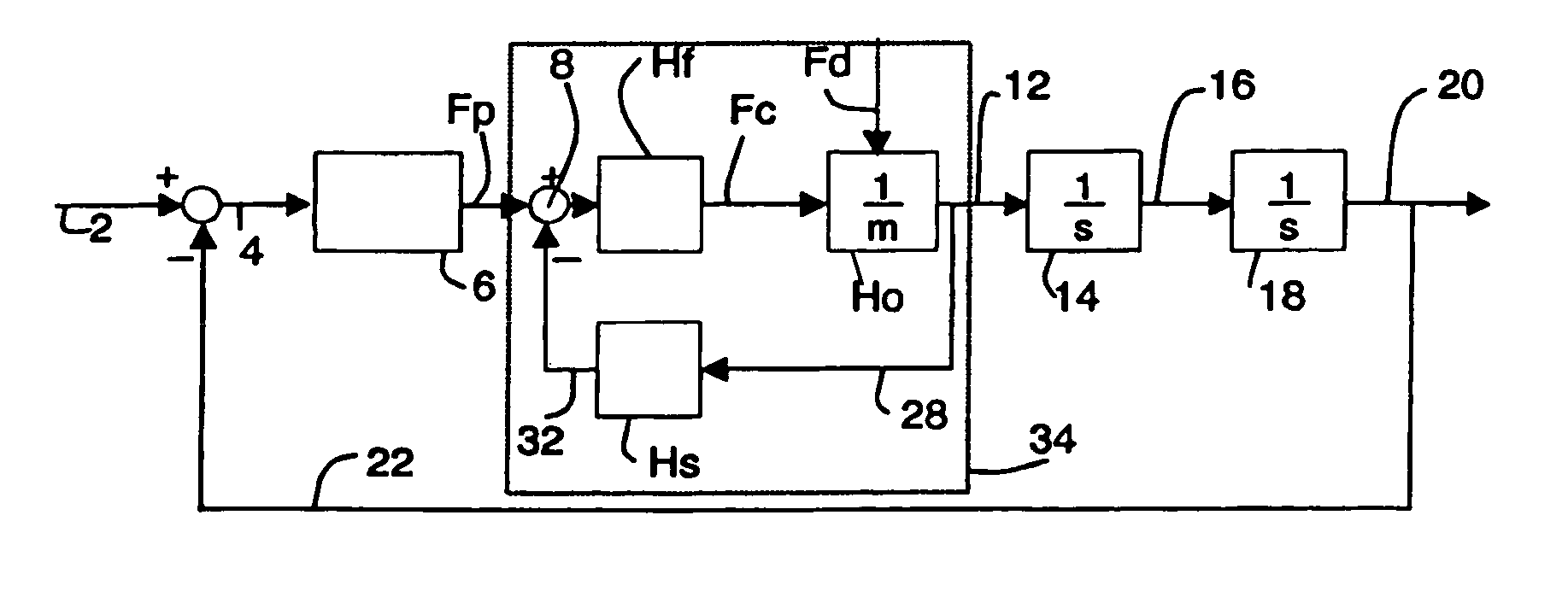
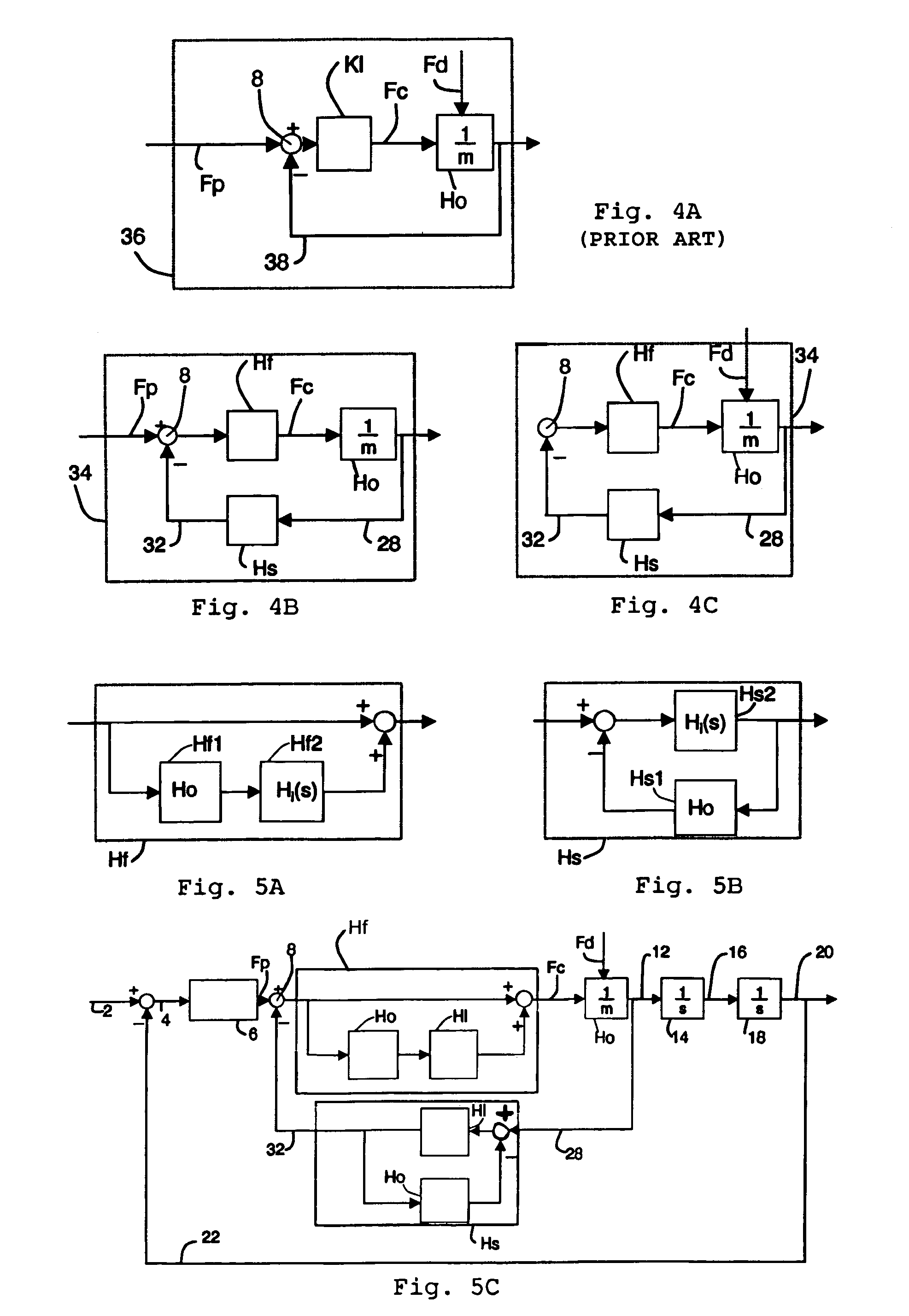
A lithographic apparatus including a position control system to control a position of a moveable object is presented, The position control system includes a position controller, an object represented as an object filter, a position feedback circuit, and an acceleration control system. The acceleration control system includes a subtractor and a first filter in a first circuit branch and a second filter in a second circuit branch. A position controller signal output from the position controller is input into the subtractor of the acceleration control system. An external disturbance force, however, is directly exerted upon the object. Thus, a first transfer function from the input of the subtractor to the acceleration of the object for the position controller force may be different than a second transfer function from the input of the object to the acceleration of the object for the disturbance force. Preferably, the first transfer function is identical to a transfer function for the position controller force in case no acceleration control system is present in the position control system.
Need to check novelty before this filing date? Find Prior Art

Description

PRIORITY INFORMATION

[0001] This application claims priority from European Patent Application No. 03077992.0, filed Sep. 22, 2003, the content of which is herein incorporated by reference in its entirety.BACKGROUND

[0002] 1. Field of the Invention

[0003] The present invention relates to lithographic apparatus and methods.

[0004] 2. Description of the Related Art

[0005] Lithographic projection apparatus can be used, for example, in the manufacture of integrated circuits (ICs). In such a case, a patterning device may generate a circuit pattern corresponding to an individual layer of the IC, and this pattern can be imaged onto a target portion (e.g. including one or more dies) on a substrate (silicon wafer) that has been coated with a layer of radiation-sensitive material (resist). In general, a single wafer will contain a whole network of adjacent target portions that are successively irradiated via the projection system, one at a time.

[0006] In the current apparatus, in which the patterning dev...

Examples

Embodiment Construction

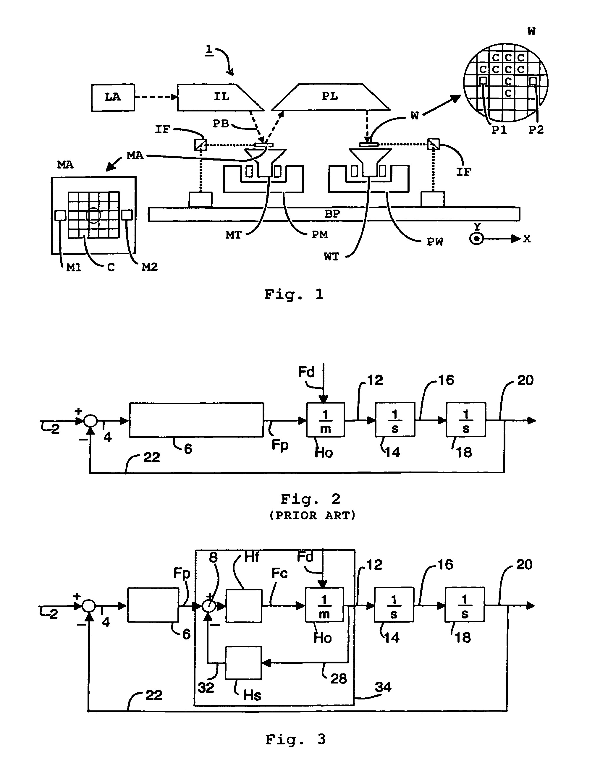
[0071]FIG. 1 schematically depicts a lithographic projection apparatus 1 according to an embodiment of the invention. The apparatus includes a radiation system IL, configured to supply a beam PB of radiation. In this particular case, the radiation system also includes a radiation source LA. The apparatus further includes a first object table (mask table) MT provided with a mask holder configured to hold a mask MA (e.g. a reticle), and connected to a first positioning device PM configured to accurately position the mask with respect to the projection system (“lens”), item PL. The apparatus also includes a second object table (substrate table) WT provided with a substrate holder configured to hold a substrate W (e.g. a resist-coated silicon wafer), and connected to a second positioning device PW configured to accurately position the substrate with respect to the projection system (“lens”), item PL, the projection system (“lens”) PL being configured to image an irradiated portion of th...