Barrier removal at low polish pressure

a technology of polishing and barriers, applied in the direction of grinding machine components, manufacturing tools, lapping machines, etc., can solve the problems of increasing the rc delay, the speed of the semiconductor device, and the crosstalk between wires and heat delay decreases, so as to achieve the effect of minimal residue, minimal seam damage, and low down for

Inactive Publication Date: 2006-09-12
APPLIED MATERIALS INC
View PDF72 Cites 27 Cited by
  • Summary
  • Abstract
  • Description
  • Claims
  • Application Information

AI Technical Summary

Benefits of technology

[0016]Embodiments of the invention generally provide methods and compositions for planarizing a substrate surface using low down force. Aspects of the invention provide compositions and methods using a combination of polishing conditions including polishing pressures, polishing compositions, various polishing speeds, selective polishing pads, and selective polishing temperatures, for removing barrier materials by a chemical mechanical polishing technique with minimal residues and minimal seam damage. Aspects of the invention are achieved by employing a strategic multi-step process comprising sequential CMP at low polish pressure to remove the deposited barrier materials.
[0019]In another embodiment, a method of chemical mechanical polishing a substrate having dielectric materials with a dielectric constant of 3.5 or less includes polishing the substrate surface by a first and second chemical mechanical polishing processes. The first and second chemical mechanical polishing processes provide a decreased polishing pressure of about 2 psi or less, an increased average platen surface speed of about 65 centimeters per second (cps) or higher, preferably about 260 cps or higher, and / or a polishing temperature of about 55° C. or higher.
[0020]In one aspect, the invention provides the use of selective polishing pads to be compatible with an increased average platen surface speed of about 195 cps or higher, and polishing the substrate surface with low down load force and thus a decreased polishing pressure of 2 psi or less.

Problems solved by technology

As semiconductor device geometries shrink to 0.13 micron or below and the speed of the semiconductor devices decreases, and cross talk between wires and heat delay increases (RC delay).
Both of these materials create challenges for processing interconnects.
Two challenges arise when using low-k dielectric materials: the mechanical hardness of low-k dielectric materials and adhesion at the interface of the low-k material and the adjacent materials.
Such undesirable structural and adhesion failures cause damage or defects as a result of aggressive processing and require the shear force or frictional force in a CMP process to be small.
Beyond 0.13 micron low-k technology, integration issues are even more difficult.
The introduction of porosity can result in substantially reduced mechanical integrity of the low-k materials and affect processing performance.
In most conventional applications, erosion and dishing are typically encountered.
Additionally, increasing the polishing pressure and increasing the polishing time to ensure copper layer removal may result in overpolishing the barrier layer and formation of topographical defects, such as concavities or depressions, referred to as dishing.
Dishing further results in a non-planar surface that impairs the ability to print high-resolution lines during subsequent photolithographic steps and detrimentally affects subsequent surface topography of the substrate and device formation.
Dishing also detrimentally affects the performance of devices by lowering the conductance and increasing the resistance of the devices, contrary to the benefit of using higher conductive materials, such as copper.
However, polishing substrates at reduced pressures often results in reduced polishing removal rates and reduced substrate throughput.
Barrier materials, such as tantalum (Ta) and tantalum nitride (TaN), are known to be chemically inert and difficult to polish at low pressure, resulting in large amounts of problematic barrier residues even after polishing by polishing compositions with high selectivity to barrier materials.
Overpolishing of the barrier residues and these protective materials by strong mechanical abrasion means metal loss, seam damage or device defect.
On the other hand, low polishing pressure processes may be unable to sufficiently remove all of the desired barrier materials from a substrate surface.
Such barrier materials or residues retained on the substrate surface can detrimentally affect device formation, such as creating short-circuits within or between devices, reducing device yields, reducing substrate throughput, and detrimentally affecting the polishing quality of the substrate surface.
On the other hand, polishing at low pressure and high velocity (e.g., 0.5 psi / 600 rpm) is commonly observed to be ineffective due to the hydroplaning effect where the removal is effectively zero.

Method used


Image

  • Barrier removal at low polish pressure
  • Barrier removal at low polish pressure
  • Barrier removal at low polish pressure

Examples


examples

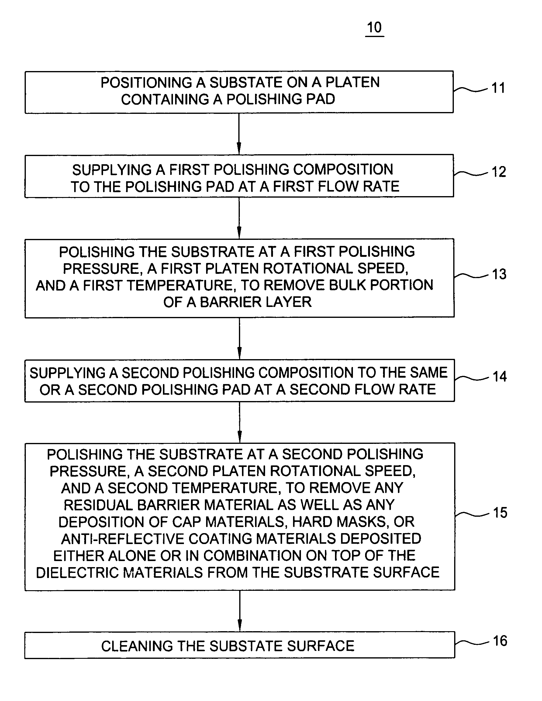
[0095]One example of features to be polished according to aspects of the invention described herein is as follows. A substrate having a low-k dielectric layer, such as Black Diamond™ from Applied Materials, Inc., of Santa Clara, Calif., with feature definitions formed therein, a tantalum or tantalum nitride barrier layer deposited on top of the dielectric layer and in the feature definitions formed therein, and a copper-containing layer deposited on the barrier layer and filling the feature definitions formed therein is provided to the polishing apparatus.

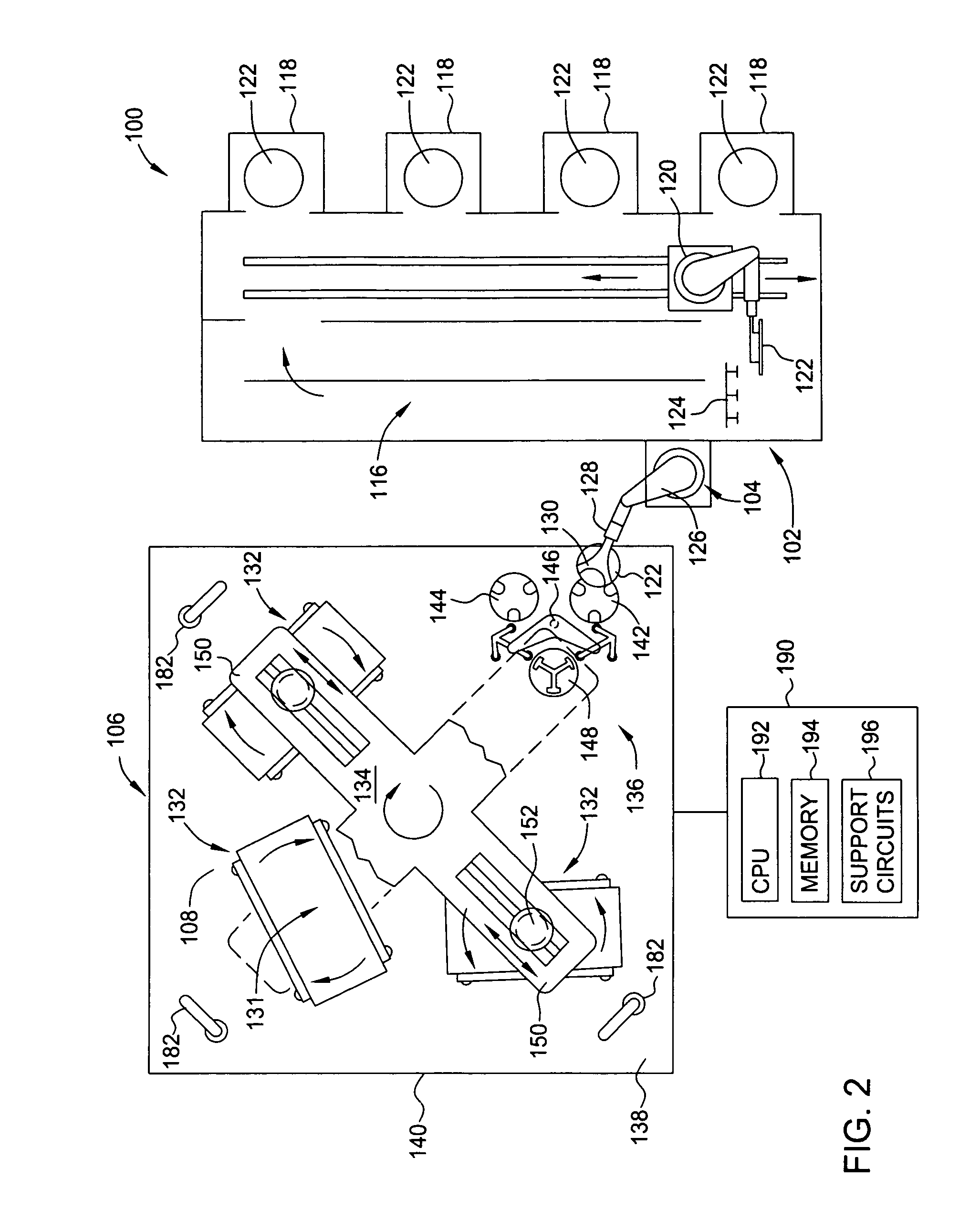
[0096]One example of the barrier removal process includes positioning a substrate on an appropriate polishing pad, such as a Politex pad available from Rodel, Inc., disposed on a web polishing platen in a Reflexion® CMP System available from Applied Materials, Inc. A first polishing composition for barrier materials is delivered to the polishing pad to remove the barrier materials and planarize the substrate surface. The first poli...


PUM

PropertyMeasurementUnit
dielectric constantaaaaaaaaaa
pressureaaaaaaaaaa
temperatureaaaaaaaaaa

Abstract

The invention generally provides methods and compositions for planarizing a substrate surface having underlying dielectric materials. Aspects of the invention provide compositions and methods using a combination of low polishing pressures, polishing compositions, various polishing speeds, selective polishing pads, and selective polishing temperatures, for removing barrier materials by a chemical mechanical polishing technique with minimal residues and minimal seam damage. Aspects of the invention are achieved by employing a strategic multi-step process including sequential CMP at low polishing pressure to remove the deposited barrier materials.

Description

CROSS-REFERENCE TO RELATED APPLICATIONS[0001]This application claims benefit of U.S. provisional patent application Ser. No. 60 / 305,314, entitled, “Dual Reducing Agents For Optimum Barrier Removal In Chemical Mechanical Polishing”, filed Jul. 13, 2001, and U.S. provisional patent application Ser. No. 60 / 353,421, entitled, “Barrier Removal at Low Polish Pressure”, filed Feb. 1, 2002. Each of the aforementioned related patent applications is herein incorporated by reference.BACKGROUND OF THE INVENTION[0002]1. Field of the Invention[0003]Embodiments of the invention generally relate to planarization of semiconductor devices and to methods and compositions for material removal using polishing techniques.[0004]2. Description of the Related Art[0005]The semiconductor industry's focus to push semiconductor performance ever faster has recently shifted from front-end device performance to back-end interconnects. The multilevel interconnects that lie at the heart of semiconductor technology r...

Claims


Application Information

Patent Timeline
Patent Type & Authority Patents(United States)
IPC IPC(8): B24B1/00H01L21/47B24B37/04B24B49/16C09G1/02H01L21/321
CPCB24B37/0056B24B37/044H01L21/3212B24B49/16C09G1/02B24B49/006
Inventor TSAI, STANMAVLIEV, RASHIDSUN, LIZHONGLIU, FENG Q.CHEN, LIANG-YUHMORAD, RATSON
Owner APPLIED MATERIALS INC
Why Eureka
Try Eureka