Energy efficient method for growing polycrystalline silicon

a polycrystalline silicon and energy-efficient technology, applied in the direction of silicon compounds, crystal growth process, condensed vapor, etc., can solve the problems of reducing the reaction rate controlling the deposition of silicon also increases, and the energy requirements to produce a unit mass of polysilicon also increase. , to achieve the effect of reducing contamination, easy to break away, and reducing the reaction rate controlling the deposition of silicon

Active Publication Date: 2006-09-12
REC SILICON
View PDF7 Cites 15 Cited by
  • Summary
  • Abstract
  • Description
  • Claims
  • Application Information

AI Technical Summary

Benefits of technology

[0020]This disclosure relates to a method for producing small polysilicon dendrites that are useful as silicon particles for charging the crucible of a crystal pulling furnace and for other purposes. These dendrites, some of which may be roughly teardrop-shaped, are produced by growing rather than by mechanically breaking. The formation of dendrites greatly reduces the electrical energy utilization as compared to growing large diameter polysilicon rods.
[0022]Dendrites can be removed from a polysilicon rod by any of several methods. By growing dendrites that have a narrow stem portion that connects the bulk dendrite to the substrate, the dendrites are easily broken away. With the dendrite stems appropriately sized, the force required to remove dendrites from the substrate is much lower than that required for producing chips from a typical polysilicon rod that is not encrusted with dendrites. The result is a reduction in contamination imparted to the polysilicon surface.
[0023]The energy required to produce dendrite polysilicon is substantially less than that required to produce conventional polysilicon. The power input to the reactor increases as the temperature is raised. However, the reaction rate controlling the deposition of silicon also increases, and therefore lowers the energy requirements to produce a unit mass of polysilicon. The kinetic effect is larger than the temperature effect resulting in an overall decrease in energy required to produce a unit mass of polysilicon. The energy reduction can approach or exceed 20 to 25%.

Problems solved by technology

However, the reaction rate controlling the deposition of silicon also increases, and therefore lowers the energy requirements to produce a unit mass of polysilicon.

Method used


Image

  • Energy efficient method for growing polycrystalline silicon
  • Energy efficient method for growing polycrystalline silicon
  • Energy efficient method for growing polycrystalline silicon

Examples


Embodiment Construction

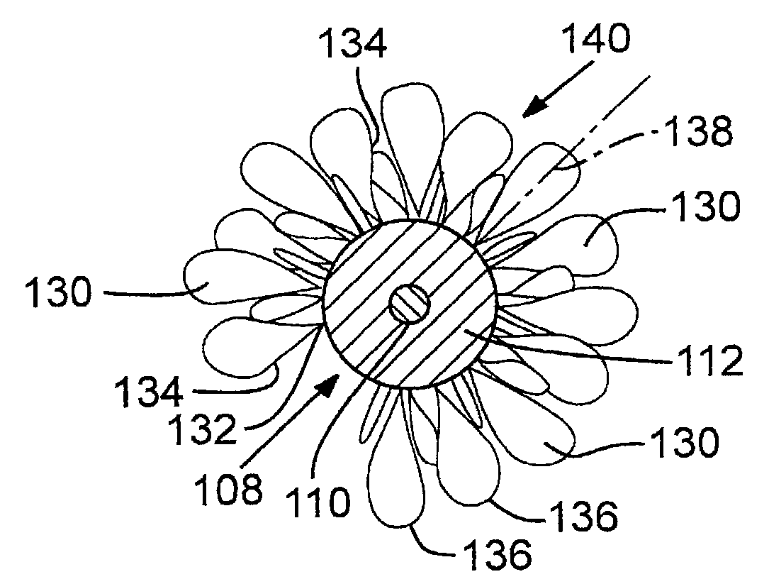
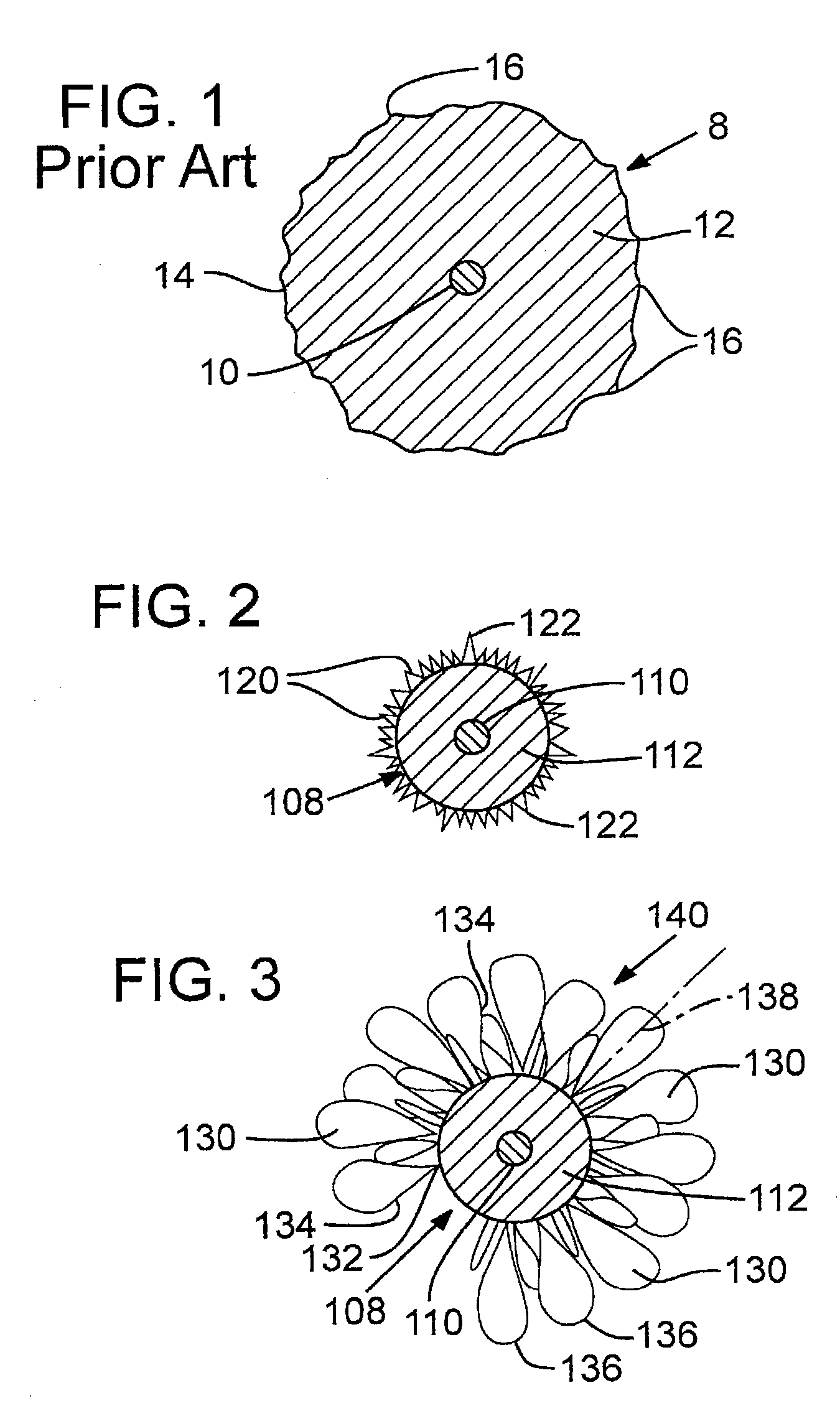
[0029]Rods grown under traditional conditions in a thermal decomposition furnace are similar to a rod 8 shown in FIG. 1 wherein a starter filament or rod 10, is covered by a continuous, generally cylindrical growth layer 12 of polycrystalline silicon. The growth layer 12 has a generally smooth exposed outer surface 14 with some rounded mounds 16.

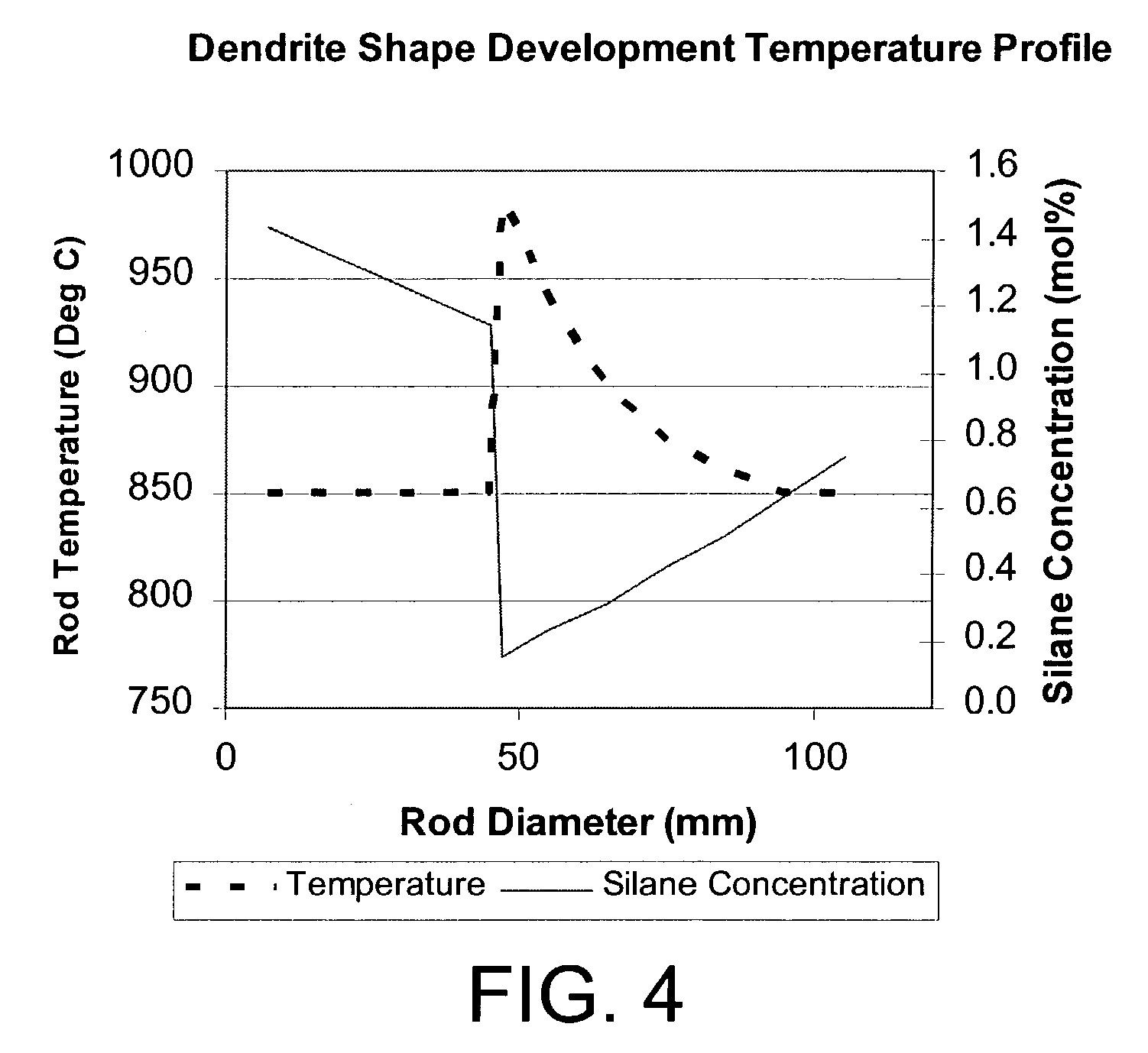
[0030]To obtain such generally smooth-surfaced rods using silane (SiH4) as the reactant gas, rod surface temperatures must be maintained on the order of 825° C. Corresponding temperatures using trichlorosilane (SiHCl3) as reactant are on the order of 1050° C. to 1100° C. Other silicon-containing compounds, such as disilane (Si2H6), trisilane (Si3H8), dichlorosilane (SiH2Cl2), silicon tetrachloride (SiCl4), dibromosilane (SiH2Br2), tribromosilane (SiHBr3), silicon tetrabromide (SiBr4), diiodosilane (SiH2I2), triiodosilane (SiHI3), and silicon tetraiodide (SiI4), each have its own optimum surface temperature for deposition. The silicon-contain...


PUM

PropertyMeasurementUnit
temperatureaaaaaaaaaa

Abstract

Polysilicon dendrites are grown by depositing silicon on a polysilicon rod or other substrate. Surface temperature is increased to a temperature at which needle-like dendrites develop due to the deposition of silicon from silicon-containing molecules in the surrounding reactor atmosphere. Thereafter, the surface temperature is gradually reduced so that silicon that deposits on the needle-like dendrites causes the dendrites to grow and assume a generally flared shape.

Description

CROSS REFERENCE TO RELATED APPLICATION[0001]This application claims the benefit of U.S. Provisional Application No. 60 / 357,212, filed Feb. 14, 2002, incorporated herein by reference in its entirety.BACKGROUND[0002]Polycrystalline silicon, or polysilicon, is a critical raw material for the electronics industry. It is the starting material for production of single-crystal silicon ingots for the semiconductor industry. These ingots are produced by either the Czochralski (CZ) or the Float Zone (FZ) method. The majority of polysilicon produced is consumed in the CZ process.[0003]In the CZ crystal-pulling process, chunks of polysilicon are loaded into a quartz crucible. The chunks of polysilicon are of random size and shape. The crucible is filled and loaded into the CZ furnace. The polysilicon is melted and a single crystal ingot is withdrawn from the melt.[0004]The yield of single crystal silicon is a function of the quantity of molten silicon that can be included within the crucible as...

Claims


Application Information

Patent Timeline
Patent Type & Authority Patents(United States)
IPC IPC(8): C30B25/12C30B25/14C01B33/029C01B33/03C01B33/035C30B25/00
CPCC01B33/035C30B25/005C30B29/06
Inventor WINTERTON, LYLE C.HILL, JOHN P.
Owner REC SILICON
Why Eureka
Try Eureka