

Light emitting device and method of manufacturing the same
a technology of light emitting devices and manufacturing methods, which is applied in the manufacture of electrode systems, electric discharge tubes/lamps, and discharge tubes luminescnet screens, etc., can solve the problems of inability to obtain el phenomenon, the efficiency of recombination of carriers is extremely poor, and the deterioration of carriers is rapidly developed, so as to reduce the manufacturing cost and improve the throughput and yield. the effect of the effect of the effect of the devi
- Summary
- Abstract
- Description
- Claims
- Application Information
AI Technical Summary
Benefits of technology
Problems solved by technology
Method used
Image

Examples
embodiment 1
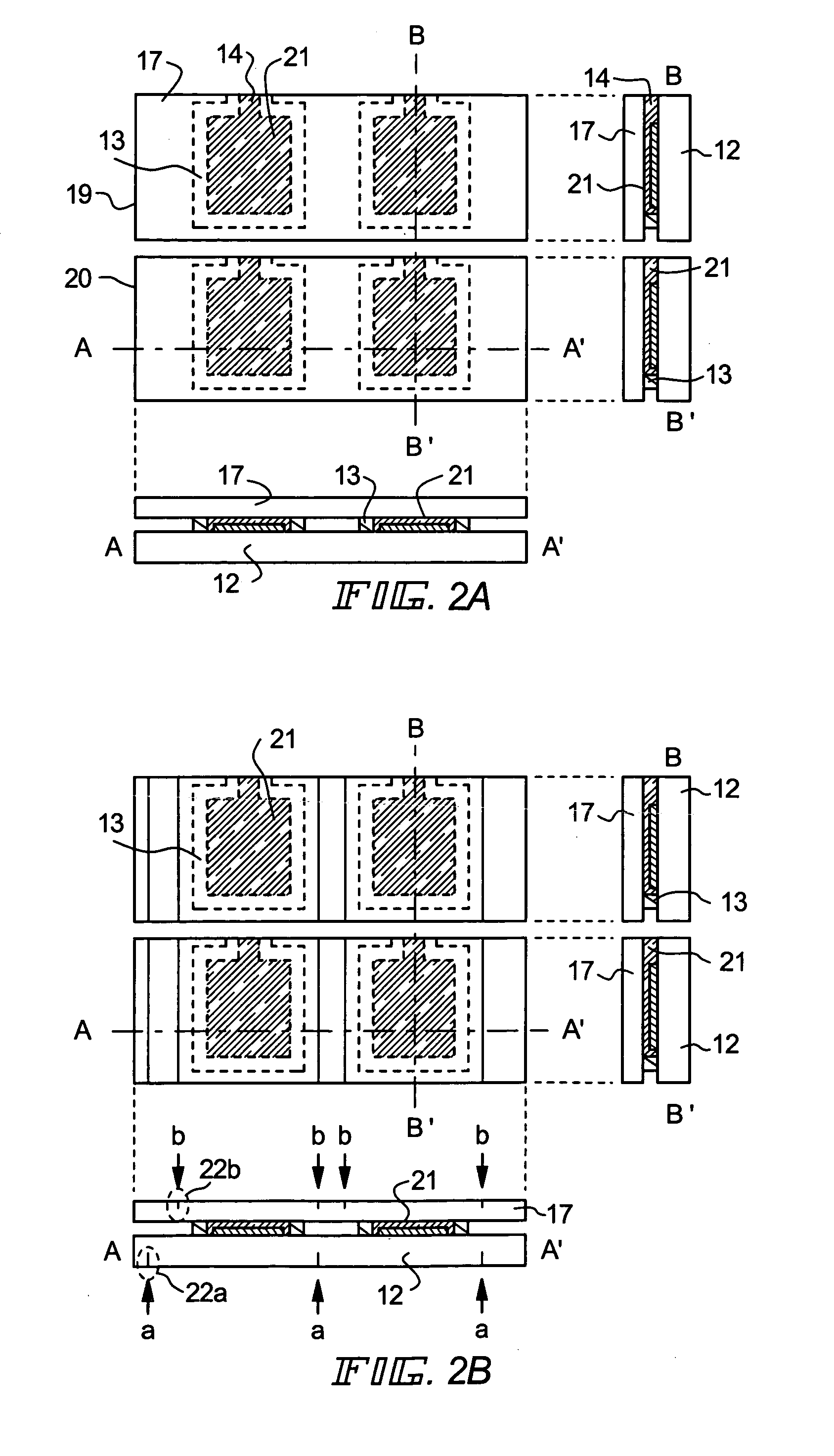
[0046]The active matrix type EL display device of the present invention will be explained in Embodiment 1 with reference to FIGS. 4(A) and 4(B). FIG. 4(A) is a top view showing the state of the device in which sealing of the EL element formed on the active matrix substrate is completed. Indicated by dotted lines, reference numeral 401 denotes a source driver circuit, 402 denotes a gate driver circuit, 403 denotes a pixel portion. Further, reference numeral 404 denotes a covering member, 405 denotes a first sealing member, and 406 denotes a second sealing member. A filler 407 (refer to FIG. 4(B)) is filled between the covering member and the active matrix substrate surrounded by the first sealing member 405.
[0047]Denoted by reference numeral 408 is a connecting wiring for transmitting a signal to be inputted to the source driver circuit 401, the gate driver circuit 402, and the pixel portion 403. The connecting wiring receives a video signal and a clock signal from an FPC (Flexible P...
embodiment 2
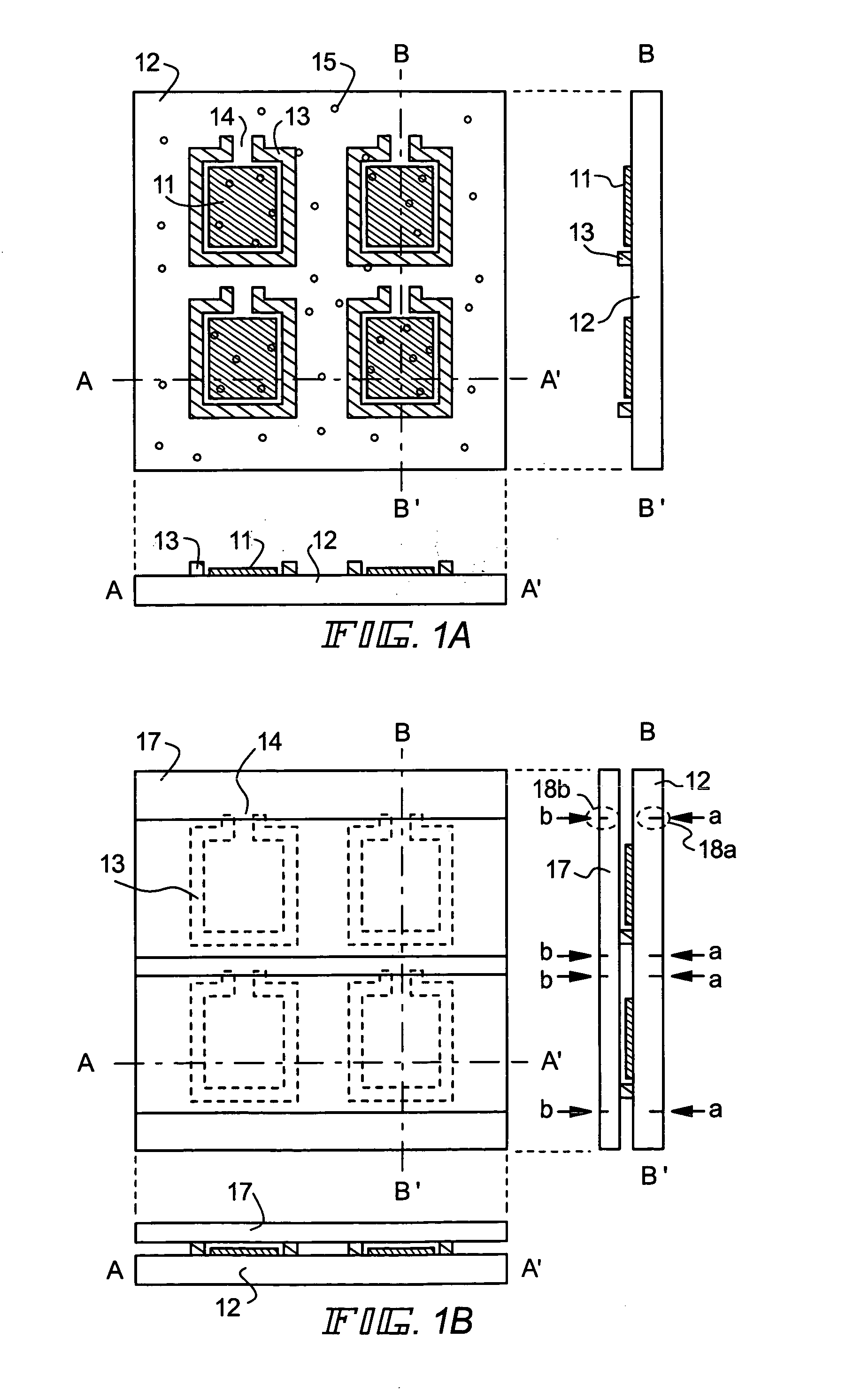
[0058]In the present embodiment, a passive matrix EL display device manufactured according to the present invention is described with reference to FIG. 5. In FIG. 5, a reference numeral 501 denotes a plastic substrate and a reference numeral 502 is a cathode formed of aluminum alloy. In the present embodiment, the cathode 502 is formed by vapor deposition. It is to be noted that, though not shown in FIG. 5, a plurality of cathodes are arranged like stripes in the direction parallel to the plane of the figure.
[0059]Further, an insulating film 503 is formed orthogonally with respect to the cathodes 502 arranged like stripes. The insulating film 503 is also provided between the cathodes 502 so as to insulate and separate the cathodes 502 from one another. Therefore, the insulating film 503 is patterned to be matrix-like when viewed from the top.
[0060]Further, a bank 504 formed of resin is formed on the insulating film 503. The bank 504 is formed in the direction perpendicular to the pl...
embodiment 3
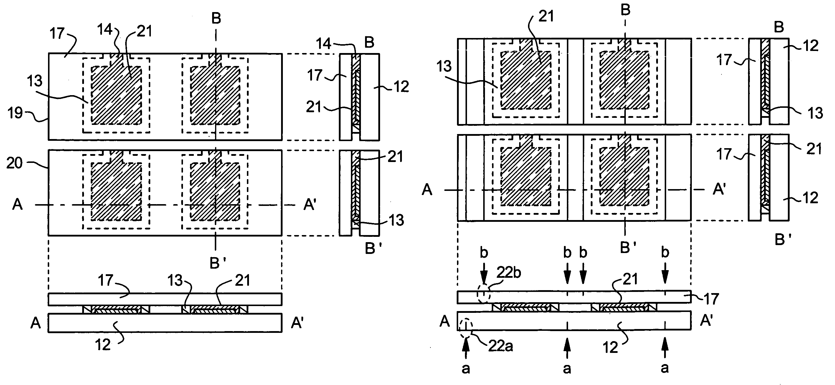
[0069]In the present embodiment, a case where encapsulant is formed in a different way from that described with reference to FIGS. 1A to 3B is described. The description is made with reference to FIGS. 6A and 6B.
[0070]In FIG. 6A, reference numerals 601, 602, and 603 denote a substrate, a pixel portion, and a first sealing material, respectively. It is to be noted that, though not shown in the figure, spacers may be scattered. As the first sealing material 603, the material of the first sealing material 13 described in the embodiment mode can be used. However, differently from the case illustrated in FIGS. 1A and 1B, in the present embodiment, no opening is provided in the first sealing material 603. More specifically, at this point, the first sealing material 603 is formed so as to form a completely closed space (so as to form a completely surrounded region).
[0071]Then, encapsulant 604 is dropped on the pixel portion 602 in the region surrounded by the first sealing material 603. Of...
PUM
 Abstract
Description
Claims
Application Information