
Strain gauges

a strain gauge and gauge body technology, applied in the direction of positive temperature coefficient thermistors, instruments, iron-filament ballast resistors, etc., can solve the problems of increasing power dissipation, requiring rather sophisticated measurement techniques, limited sensitivity of metal wire and foil gauges, etc., to achieve high sensitivity, scalable and economic

Inactive Publication Date: 2006-10-03
COMMONWEALTH SCI & IND RES ORG +1
View PDF23 Cites 27 Cited by
  • Summary
  • Abstract
  • Description
  • Claims
  • Application Information

AI Technical Summary

Benefits of technology

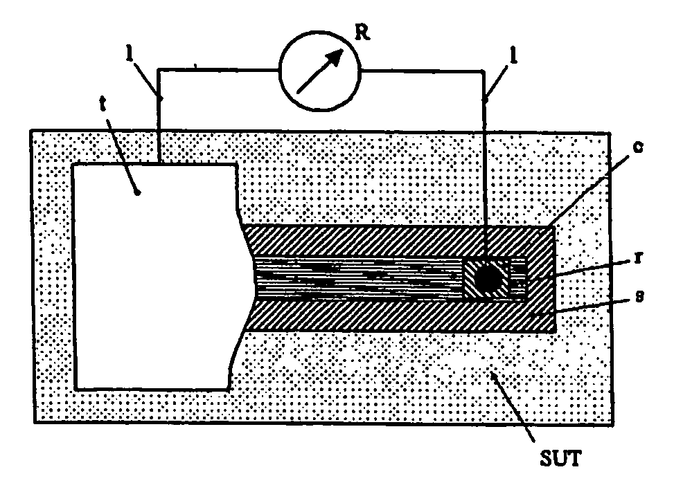
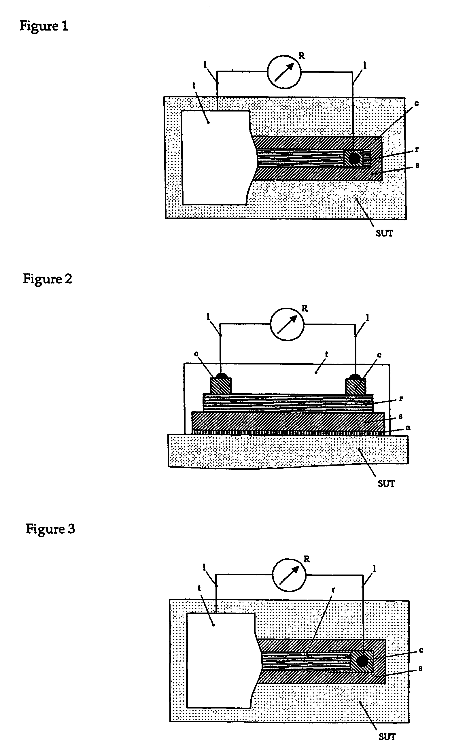
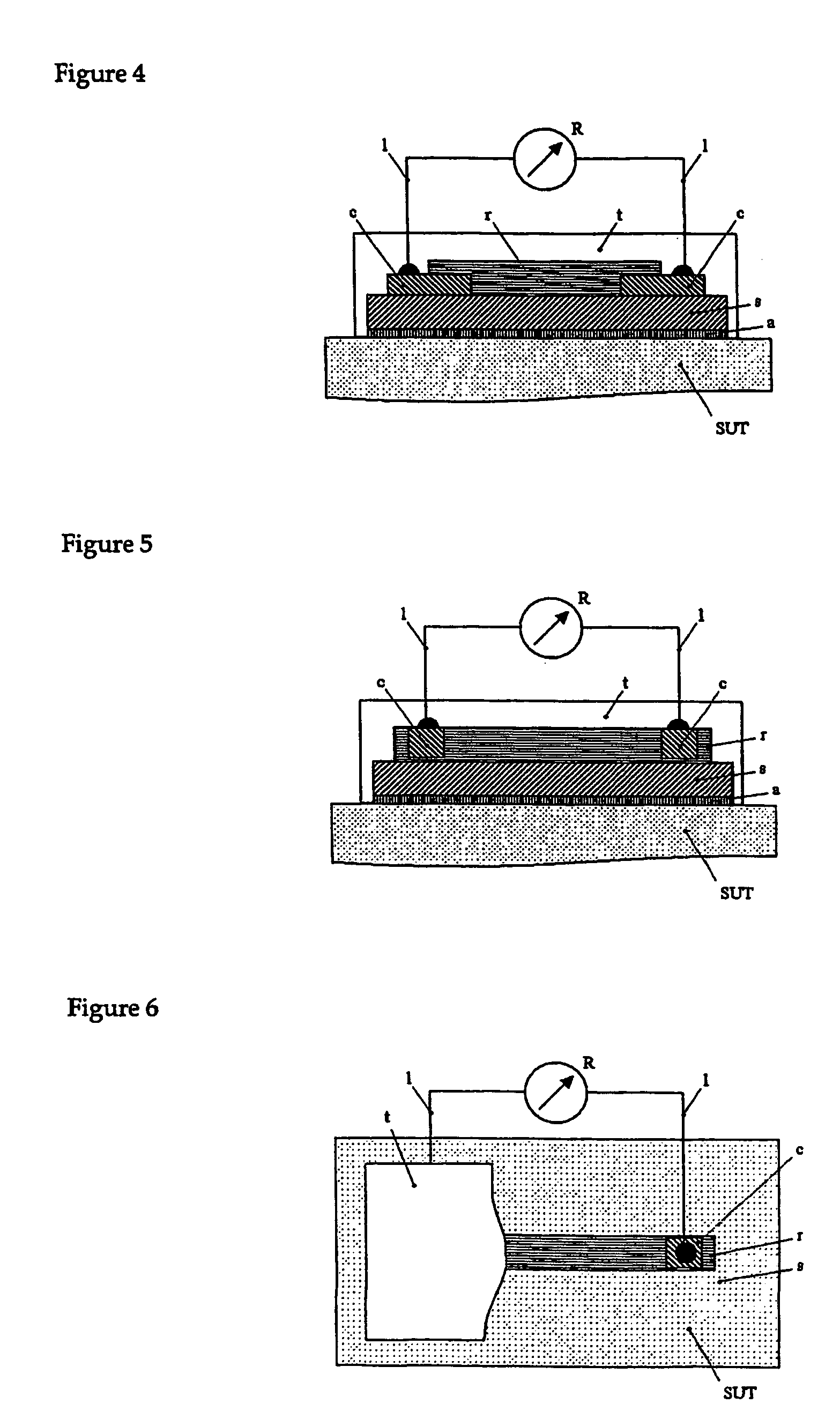
[0008]In the strain gauge of the present invention the resistive layer comprises metallic or semiconducting nanoparticles or aggregates thereof which are separated by insulating or semiconducting barriers. The conduction in the nanoparticle layer is governed by tunnelling between nanoparticles through these barriers. When the layer is deformed due to the application of an external mechanical load, the separation between the nanoparticles changes. Correspondingly, the tunnelling current and thus the resistance of the layer changes. The exponential dependence of the tunnelling current on the thickness of the tunnel barrier results in the high sensitivity of the gauges, which can be almost two orders of magnitude higher than that of metal foil gauges and is comparable to that of semiconductor-based gauges.
[0012]The nanoparticle layer can be produced by a variety of deposition techniques. Clearly it is preferable to use a deposition process which is reproducible and controllable, capable of producing homogeneous films based on a variety of nanoparticle types, capping agents and cross-linkers on different surfaces (specifically, on flexible substrates), and is rapid, scalable and economic. One such method was developed to form nanoparticle films on nanoporous substrates (Raguse et al., WO 01 / 25316). An alternative process produces stable concentrates of functionalised nanoparticles or cross-linked nanoparticle aggregates as inks for printing, spraying, drawing and painting processes, where the nanoparticles are functionalised with organic molecules or inorganic compounds. In this process, the nanoparticles or cross-linked aggregates of nanoparticles are coated with a protecting layer of organic molecules or inorganic compounds to halt aggregation of the nanoparticles or aggregates. Sols of the functionalised nanoparticles or aggregates of nanoparticles are concentrated using methods such as centrifugation, filtration, dialysis or precipitation, either once or repeatedly. During the concentration process residues, pollutants and excess protectant or cross-linker molecules are removed from the nanoparticle sols. The resulting concentrates can be printed, sprayed, painted or drawn to produce coherent nanoparticle films on rigid and flexible substrates.
[0013]Besides their high sensitivity, a further advantage of the nanoparticle layers compared to metallic films is their resistivity, which can be several orders of magnitude higher than that of metallic conductors. The higher resistance of the nanoparticle films is advantageous for several reasons. The power dissipation is reduced, since for a constant measuring voltage the power is inversely proportional to the resistance. As a result, higher excitations can be used or, alternatively, the length of the resistive path can be reduced. This means that either the sensor dimensions can be made smaller or that there is no need for patterning meandered structures. In either case, the spatial resolution of the strain measurement is improved. This facilitates the deposition of multiple strain gauges for the measurement of the in-plane strain components, and of arrays of strain gauges for mapping the strain distribution on the surface of structures and for similar non-destructive evaluation tasks.

Problems solved by technology

Metal wire and foil gauges have a limited sensitivity, which means that rather sophisticated measurement techniques are required to detect relative changes in resistance as low as a few ppm corresponding to low strains in the microstrain range.
Furthermore, the resistivity of the conductor material of such gauges is rather low, resulting in increased power dissipation.
This places restrictions on the minimum size of the gauge structure and thus on the spatial resolution of the strain measurements.
Semiconductor-based gauges, on the other hand, while exhibiting higher sensitivities, suffer from non-linear behaviour, high temperature coefficients of resistivity, low strain limits and a complex (and thus costly) manufacturing process.

Method used


Image

  • Strain gauges
  • Strain gauges
  • Strain gauges

Examples


example 1

[0042]A tunnel strain gauge was produced using a nanoparticle film based on a functionalised nanoparticle concentrate consisting of gold nanoparticles with an average diameter of 18 nm which were surrounded by self-assembled capping layers of 4-nitrothiophenol (4-NTP). The film was sprayed onto an ink jet transparency with a thickness of 0.14 mm as a substrate using an airbrush.

[0043]Thin gold wires (diameter 0.05 mm) were attached to the film using silver paint in order to connect the gauge to an Ohmmeter. The separation between the contacts was 6 mm, and the width of the gauge film was 5 mm. Since the room temperature resistance of the unstrained gauge was ca. 250 kΩ and the resistance of the leads was of the order of 1 Ω, a two-point resistance measurement was sufficient.

[0044]To assess the sensitivity of the nanoparticle tunnel strain gauge, the gauge was attached to surfaces with different radii of curvature, thus exposing the gauge to varying bend strains. Both compressive and...

example 2

[0045]A tunnel strain gauge was produced using a nanoparticle film deposited with the technique described by Raguse et al. (WO125316A1, 2001). The film consisted of gold nanoparticles with an average diameter of 8 nm which were cross-linked by C2-dithiol. The film was deposited onto a nanoporous fluoropolymer (PVDF) membrane with a thickness of 0.14 mm as a substrate using a filtration method.

[0046]Thin gold wires (diameter 0.05 mm) were attached to the film using silver paint in order to connect the gauge to an Ohmmeter. The separation between the contacts was 7 mm, and the width of the gauge film was 3 mm. Since the room temperature resistance of the unstrained gauge was ca. 3 MΩ and the resistance of the leads was of the order of 1 Ω, a two-point resistance measurement was sufficient.

[0047]To assess the sensitivity of the nanoparticle tunnel strain gauge, the gauge was attached to surfaces with different radii of curvature, thus exposing the gauge to varying bend strains. Both co...

example 3

[0048]A tunnel strain gauge similar to the one described in example 1 was produced; however, the nanoparticle concentrate was based on silver nanoparticles with an average diameter of 50 nm instead of gold nanoparticles as in example 1. FIG. 13 shows the measured resistance change as a function of the bend strain. The gauge factor G=ΔR / R / ε is about 60.


PUM

PropertyMeasurementUnit
sizeaaaaaaaaaa
particle diametersaaaaaaaaaa
sizesaaaaaaaaaa

Abstract

The present invention provides a strain gauge comprising a resistive layer. The resistive layer comprises metallic or semiconducting nanoparticles or aggregates thereof in which the nanoparticles or aggregates thereof are separated by insulating and / or semiconducting material.

Description

[0001]This application is the U.S. National Phase of International Application PCT / AU02 / 01133, filed 26 Aug. 2002, which designated the U.S.FIELD OF THE INVENTION[0002]The present invention relates generally to the construction of strain gauges, and more particularly to highly sensitive and compact strain gauges based on films containing nanoparticles.BACKGROUND OF THE INVENTION[0003]Strain gauges measure the change in resistance of an electrical conductor associated with the application of a mechanical load to the conductor which results in a strain. This change in resistance can be due to changes in the geometry of the conductor and in the resistivity of the conductor material. Conventional strain gauges are based on metallic wires or foils or on micromachined single- or polycrystalline semiconductors. These gauges are usually attached to a flexible plastic substrate, which in turn is bonded to the structure for which the strain has to be determined. The sensitivity of a strain ga...

Claims


Application Information

Patent Timeline
Patent Type & Authority Patents(United States)
IPC IPC(8): G01L1/22B32B7/02G01L1/20
CPCG01L1/2293
Inventor HERMANN, JANRAGUSE, BURKHARDREDA, TORSTENWILSON, ALAN RICHARD
Owner COMMONWEALTH SCI & IND RES ORG
Learn More