Electrostatic drive type MEMS device and manufacturing method thereof, optical MEMS device, light modulation device, GLV device, and laser display

a technology of drive type and drive device, which is applied in the direction of optical elements, coatings, instruments, etc., can solve the problems of uneven surface transcribed surface of side electrodes, uneven reflectance, uneven surface of piled-up electrodes, etc., and achieve the effect of improving the flatness of the overall chip having the mems device, improving the performance of the mems device, and improving the degree of packaging freedom

Inactive Publication Date: 2006-10-03
SONY CORP
View PDF7 Cites 22 Cited by
  • Summary
  • Abstract
  • Description
  • Claims
  • Application Information

AI Technical Summary

Benefits of technology

[0043]According to an electrostatic drive type MEMS device of the present invention, since a substrate side electrode is formed of an impurities-doped conductive semiconductor region in a semiconductor substrate, and the surface of the substrate side electrode is maintained as the same flattened surface as the surface of the semiconductor substrate, surface unevenness (roughness) of a driving side electrode of a beam, which has become obvious in the MEMS device, can be extremely reduced and flattened as well. As a result, improvements in the performance of the MEMS device can be obtained. Further, since the substrate side electrode of the MEMS device is formed on the same surface as the surface of the semiconductor substrate, the flatness of an overall chip having the MEMS device is improved, the degree of freedom of packaging that is unique to the MEMS device is increased, the degree of freedom in designing a manufacturing process can be improved, and reduction of costs can be implemented.
[0044]According to manufacturing methods of an electrostatic drive type MEMS device of the present invention, it is possible to manufacture the above-mentioned MEMS devices easily and accurately.
[0045]When an electrostat...

Problems solved by technology

However, since these materials have a crystalline structure, unevenness occurs on the surface thereof.
This surface unevenness does not pose a serious problem in terms of the electric characteristics as well as the operating characteristics of the MEMS device, but it often has become problematic in the manufacturing process of an optical MEMS device.
In this case, surface unevenness of a lower layer film becomes sequentially transcribed to an upper layer film in the manufacturing process, thereby resulting in the forming of a driving side electrode with piled-up transcribed surface unevenness, that is, the forming of a reflective film therewith on the uppermost layer that is an optically important film surface.
However, if there is no control on the amount of this surface unevenne...

Method used


Image

  • Electrostatic drive type MEMS device and manufacturing method thereof, optical MEMS device, light modulation device, GLV device, and laser display
  • Electrostatic drive type MEMS device and manufacturing method thereof, optical MEMS device, light modulation device, GLV device, and laser display
  • Electrostatic drive type MEMS device and manufacturing method thereof, optical MEMS device, light modulation device, GLV device, and laser display

Examples


Embodiment Construction

[0066]Hereinafter, the embodiments of the present invention will be explained with reference to drawings.

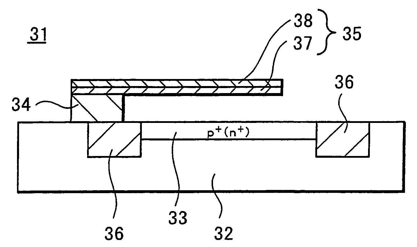
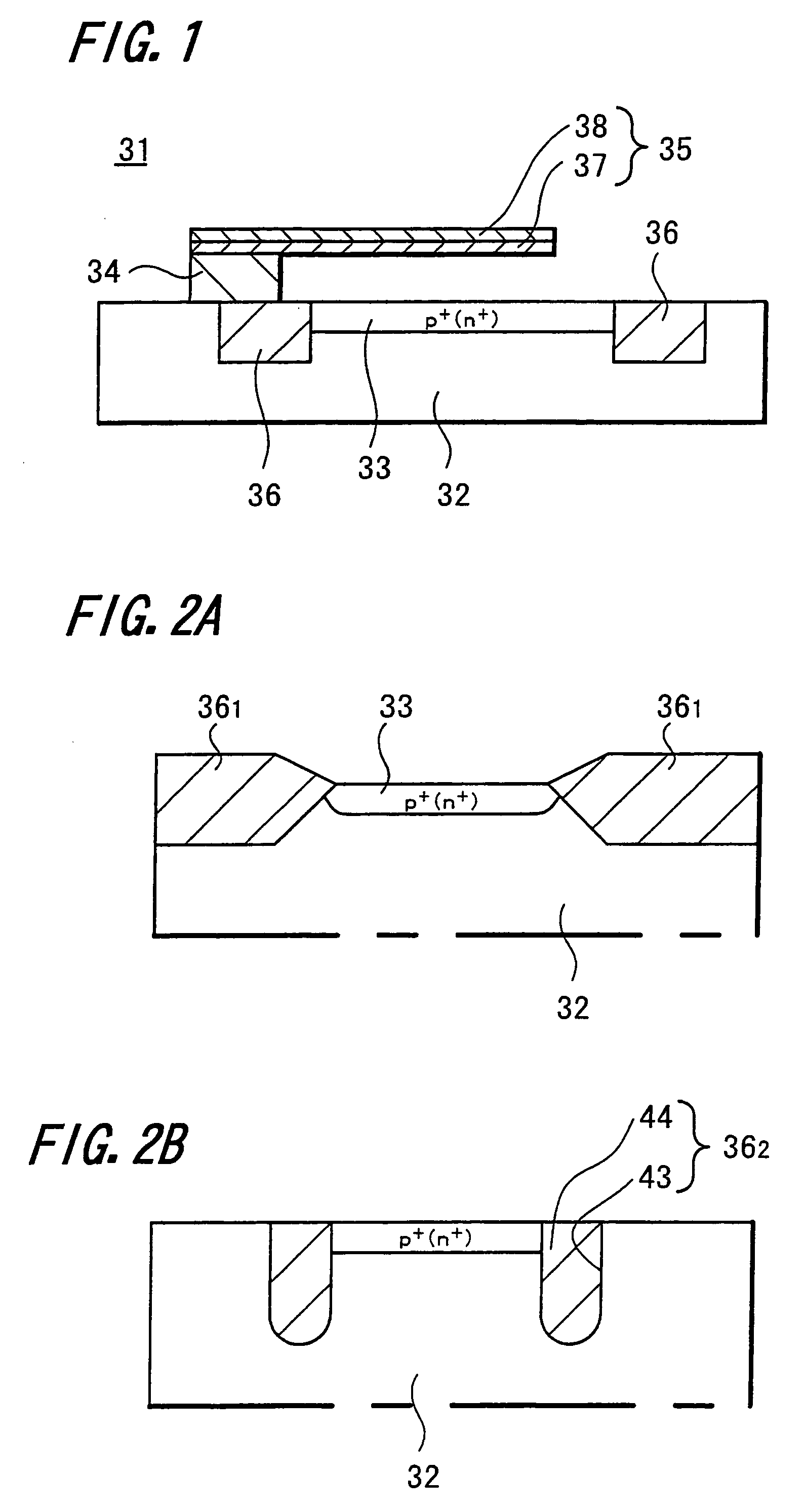
[0067]FIG. 1 shows one typical embodiment of an electrostatic drive type MEMS device according to the present invention.

[0068]A MEMS device 31 according to the present invention is composed by forming a conductive semiconductor region 33 in a predetermined region of one surface of a semiconductor substrate 32 with the required doping of conductive type impurities, and after the conductive semiconductor region 33 is made to be a substrate side electrode, by disposing an electrostatic drive type beam 35, one end of which is supported by an insulative support part 34 so as to oppose the substrate side electrode 33. The beam 35 is composed in a so-called cantilever fashion. Meanwhile, a semiconductor integrated circuit and the like to control the driving is incorporated into a part of the MEMS device 31.

[0069]A substrate consisting of, for example, silicon (Si), gallium arsenic (GaAs...


PUM

PropertyMeasurementUnit
Forceaaaaaaaaaa
Electrical conductoraaaaaaaaaa
Strengthaaaaaaaaaa

Abstract

An electrostatic drive type MEMS device and a manufacturing method thereof are provided, in which flattening the surface of a driving side electrode, improving performance, and furthering the improvements of the degree of freedom of designing in the manufacturing process are implemented. In addition, a GLV device using this MEMS device is provided, and further a laser display using this GLV device is also provided. The electrostatic drive type MEMS device includes a substrate side electrode and a beam having a driving side electrode driven by electrostatic attraction force or electrostatic repulsion force that acts between the substrate side electrode and driving side electrode, in which the substrate side electrode is formed of an impurities-doped conductive semiconductor region in a semiconductor substrate.

Description

TECHNICAL FIELD[0001]The present invention relates to an electrostatic drive type MEMS device and a manufacturing method thereof, an optical MEMS device, a light modulation device, a GLV device and a laser display.BACKGROUND ART[0002]With the advances in microscopic manufacturing technology, much attention has been focused on so-called micro-machine (MEMS: Micro Electro Mechanical Systems, ultra-miniature electric, mechanical compound) devices and miniature devices in which MEMS devices are incorporated.[0003]A MEMS device is a device that is formed on a substrate such as a silicon substrate, glass substrate or the like as a microscopic structure, and electrically and further, mechanically unites a driving body outputting mechanical driving force with a semiconductor integrated circuit or the like that controls the mechanical body. A basic feature of the MEMS device is that a mechanically structured driving body is incorporated in a part of the device, and the driving body is electr...

Claims


Application Information

Patent Timeline
IPC IPC(8): G02B26/00B81B3/00G02B26/02B81C1/00G02B5/18G02B26/08
CPCB81C1/0015G02B26/0841B81B2201/045B81B2203/04B81C2201/0109B81C2201/0173B81C2203/0109B81B3/00B81C1/00G02B5/18G02B26/02
Inventor IKEDA, KOICHI
Owner SONY CORP
Why Eureka
Try Eureka