Method of generating multiple oxides by plasma nitridation on oxide

a plasma nitridation and oxide technology, applied in the direction of semiconductor devices, electrical equipment, basic electric elements, etc., can solve the problems of large standby power consumption, low production efficiency, and low efficiency of products with these devices, so as to reduce leakage current, minimize corner rounding, and reduce the effect of little or no effect on the integrity of the sti region

Inactive Publication Date: 2006-10-10
TAIWAN SEMICON MFG CO LTD
View PDF16 Cites 22 Cited by
  • Summary
  • Abstract
  • Description
  • Claims
  • Application Information

AI Technical Summary

Benefits of technology

[0014]A still further objective of the present invention is to provide a method of forming multiple gate oxide thicknesses that has little or no effect on the integrity of the STI regions in the device, especially minimizing corner rounding that occurs with etch back methods.
[0015]A still further objective is to reduce the leakage current across the thin gate oxide layers in the resulting MOSFET to avoid degradation in device performance.
[0016]These objectives are achieved by first providing a substrate with active areas separated by regions of insulating material such as STI features. In the first embodiment where a triple oxide thickness is generated, a first layer of silicon dioxide is grown on the active areas. Some regions of the oxide layer are selectively removed by patterning a photoresist layer on the substrate and then etching away the oxide that has been exposed through openings in the photoresist layer. The photoresist is stripped and a second oxide layer is grown on the active areas. The second oxide layer is thinner than the first oxide layer and the second growth adds to the oxide thickness in first growth areas that have not been removed by etching. In first growth regions where the oxide was previously removed by etching, the second growth forms a thinner oxide thickness than was removed by the previous etch. A photoresist is then patterned on the substrate to selectively expose some of the second growth regions. A plasma nitridation is performed which introduces nitrogen into the second growth oxide regions that are uncovered in the photoresist pattern. The nitridation reduces the effective oxide thickness of the second growth gate oxide relative to second growth regions that are not subjected to nitridation. The photoresist is stripped and the substrate is ready for further processing. An annealing step can be performed to remove moisture and contaminants from the substrate and to densify the gate oxides into more uniform layers. As a result, there are three effective oxide thicknesses formed. The thinnest oxide layer contains nitrogen which prevents mobile impurities such as boron from migrating between the underlying channel and the gate electrode once the device fabrication is complete. Another advantage is that the number of etch steps has been reduced from two in prior art to one. This reduces the corner rounding damage to the STI features.
[0017]In a second embodiment, multiple oxide layers involving four different oxide thicknesses are generated. The first embodiment is followed to the point where a photoresist is selectively patterned over the first and second oxide growth regions. In this case, some of both first and second growth regions are uncovered by the photoresist pattern. Nitridation of the uncovered first and second oxide growth regions reduces the effective oxide thickness in these areas relative to the first and second oxide growth regions that are protected by photoresist. The photoresist layer is then removed, and the substrate is cleaned and annealed. The substrate is ready for subsequent processing in which the gate electrode and source/drain regions are formed. As a result, there are four different effective gate oxide thicknesses on the sub

Problems solved by technology

One concern associated with a thin gate oxide is that it will not be thick enough to prevent migration of impurities such as boron dopant from occurring between the gate electrode and channel regions which will degrade the device performance.
This will cause a large current in the standby mode (IOFF) and a large standby power consumption, thereby making products with these devices commercially unacceptable.
Another concern associated with thin gate oxides is that an excessively high voltage applied to the gate electrode can cause a gate breakdown resulting in a short circuit between the gate electrode and source region.
A thicker gate oxide will allow a higher breakdown voltage but at the expense o

Method used


Image

  • Method of generating multiple oxides by plasma nitridation on oxide
  • Method of generating multiple oxides by plasma nitridation on oxide
  • Method of generating multiple oxides by plasma nitridation on oxide

Examples


second embodiment

[0046]In a second embodiment, the present invention is a method of forming four different gate oxide thicknesses on a substrate which is useful in fabricating semiconductor devices that have several functions or systems on a chip (SOC) wherein different types of circuits requiring different gate oxide thicknesses are needed. This embodiment is represented in FIGS. 4a–4d. First, a substrate 40 is provided which contains STI regions 41 that separate active areas where circuits will be formed. A first growth oxide layer 42a is grown to a thickness of about 50 Angstroms preferably in an oxidation furnace with a dry oxygen ambient at a temperature of 600° C. to 800° C. for a period of 20 minutes as in the previous embodiment. A photoresist layer 43 is then patterned to selectively expose portions of oxide layer 42a that will be removed and replaced with an oxide layer having a lower EOT than oxide 42a.

first embodiment

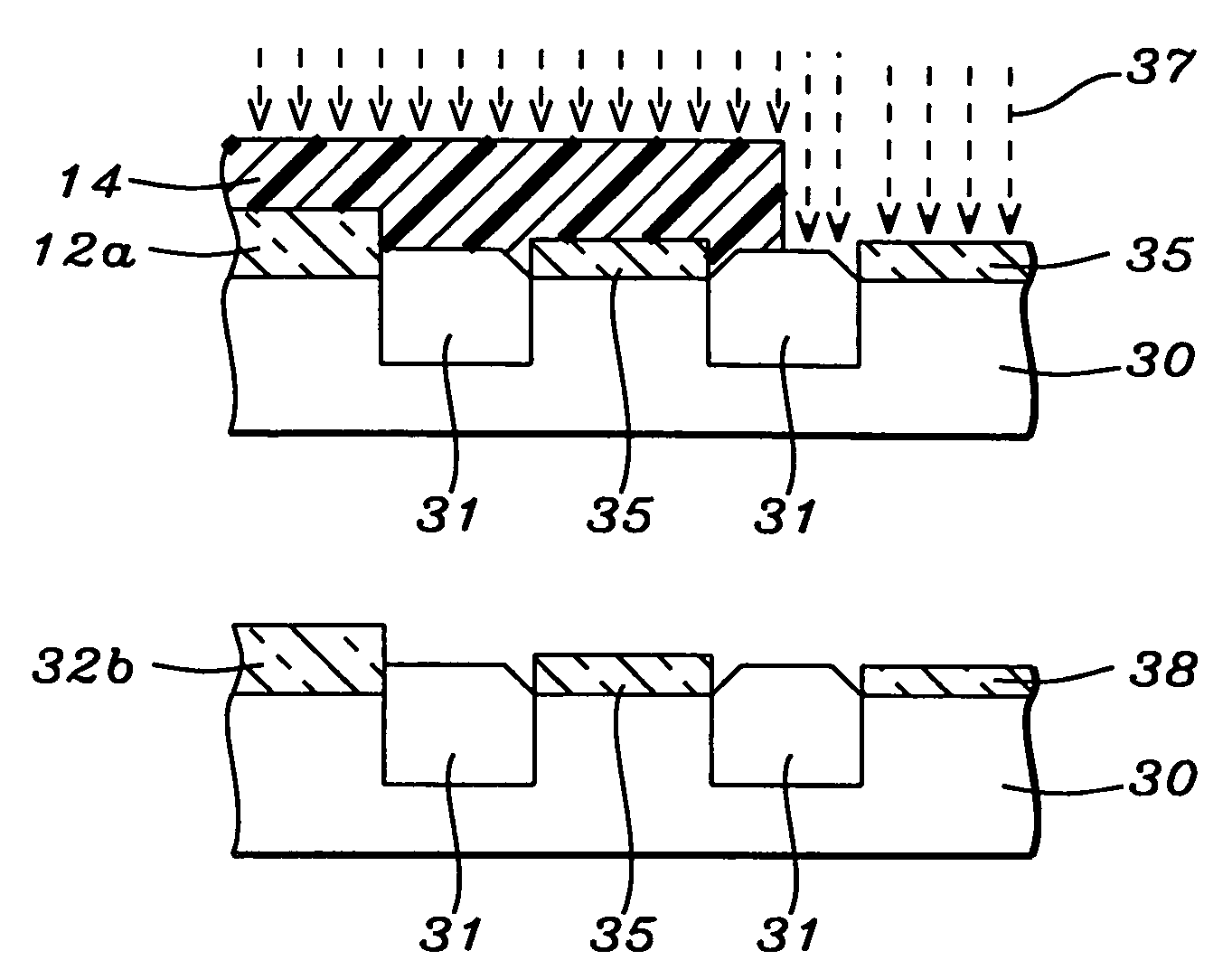
[0047]Referring to FIG. 4b, the exposed oxide regions 42a are etched away in dilute HF as described previously. Comers of STI regions 41 exposed to the etchant can become rounded during the treatment. Photoresist 43 is removed with a liquid stripper and substrate 40 is cleaned with SC-1 and SC-2 solutions as mentioned in the An annealing step may be performed here to remove moisture and contaminants and to density any native oxide growth that can occur on substrate 40 after the strip process. A second oxide layer 44 about 20 Angstroms thick is then grown on substrate 40 in regions where oxide layer 42a was previously removed. In regions where oxide 42a remains in FIG. 4a, the second oxide growth adds slightly to the thickness to give oxide layer 42b about 55 to 60 Angstroms thick.

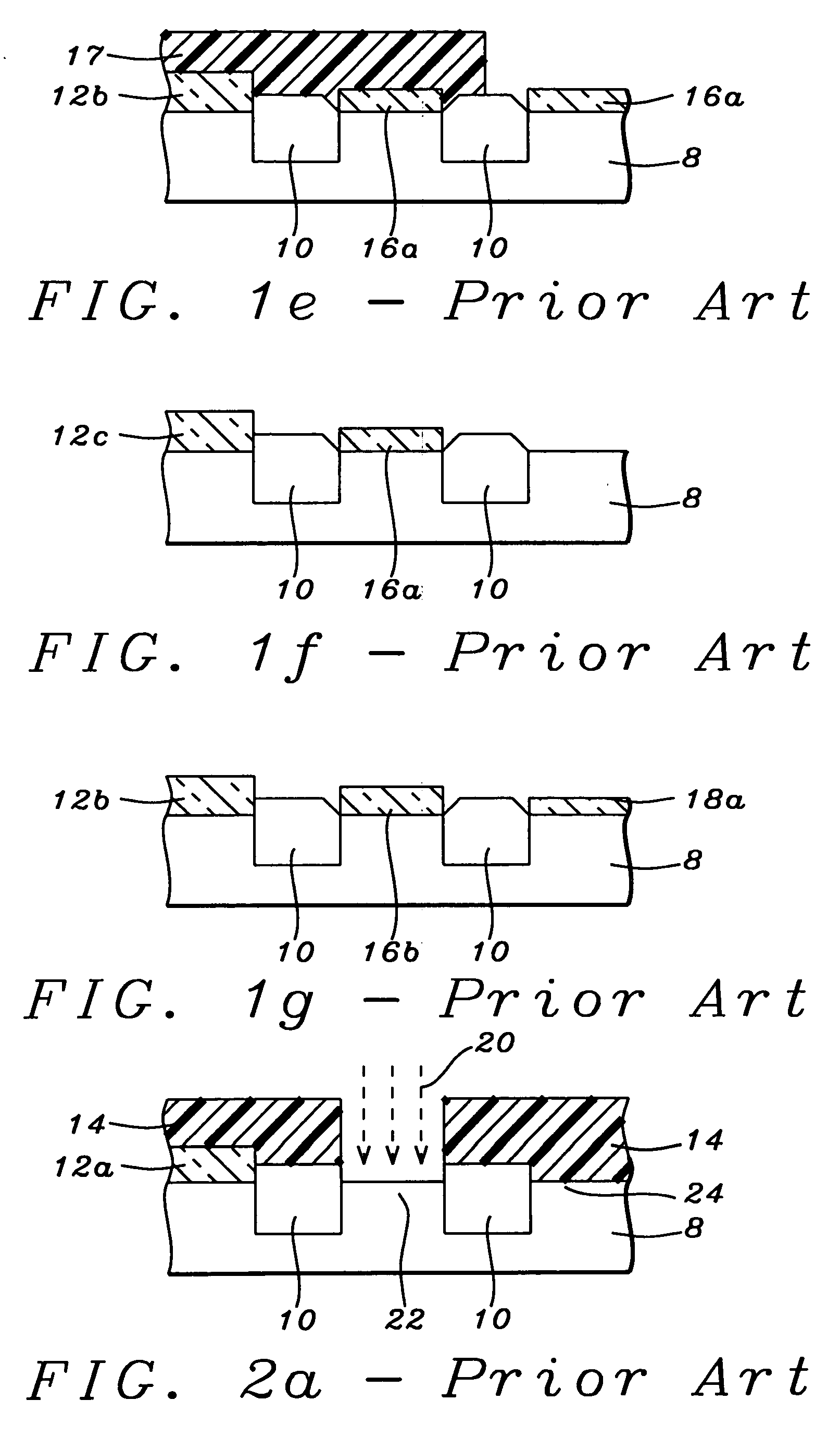
[0048]Referring to FIG. 4c, a photoresist layer 45 is patterned to expose selected oxide layers 42b, 44 while covering other oxide layers 42b, 44. A nitridation 46 with nitrogen plasma as described in the ...

third embodiment

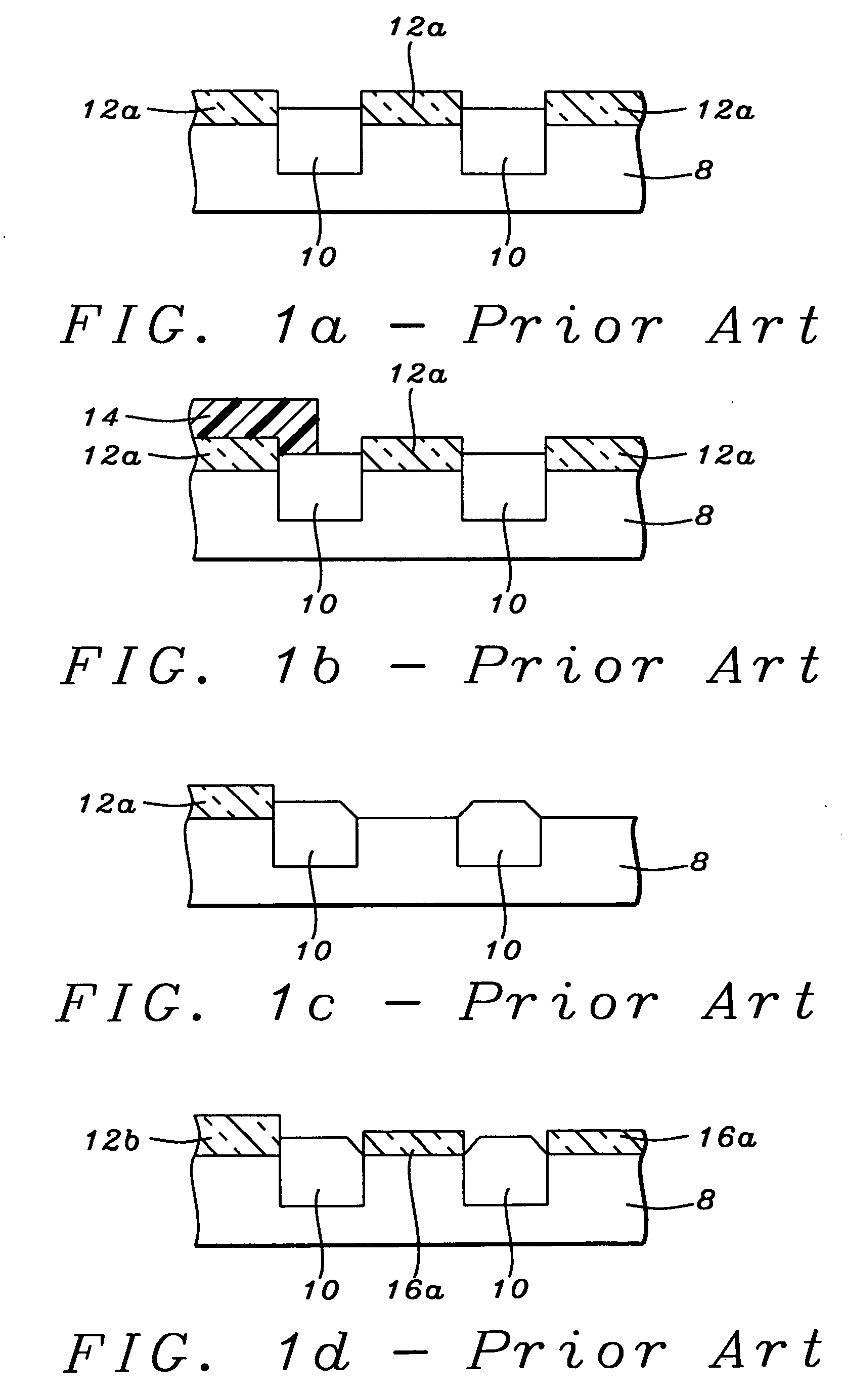
[0051]In a third embodiment, the etch back step described for FIGS. 4a–4b is shortened to 10 seconds and a regrowth of oxide is omitted. Exposed oxide layer 42a in FIG. 4a is selectively etched by dilute HF as before but the etch time is shortened to 10 seconds so that exposed oxide layer 42a is thinned to about 20 Angstroms thick to form oxide layer 50 in FIG. 5a. As a result there is little or no corner rounding of STI features 41 adjacent to oxide layer 50 during the etch process. Oxide layer 42a remains 50 Angstroms thick.

[0052]Photoresist 43 is removed and substrate 40 is cleaned by conventional methods. Referring to FIG. 5b, a photoresist 51 is patterned to selectively expose oxide layers 42a, 50 and to cover other selected layers 42a, 50. A nitridation 52 is then performed as described in the first embodiment. Oxide layers 42a, 50 that are not protected by photoresist 51 are nitridated to form layers 53, 54, respectively.

[0053]Referring to FIG. 5c, nitridated oxide layer 53 i...


PUM


Abstract

A method of forming multiple gate oxide thicknesses on active areas that are separated by STI isolation regions on a substrate. A first layer of oxide is grown to a thickness of about 50 Angstroms and selected regions are then removed. A second layer of oxide is grown that is thinner than first growth oxide. For three different gate oxide thicknesses, selected second oxide growth regions are nitridated with a N2 plasma which increases the dielectric constant of a gate oxide and reduces the effective oxide thickness. To achieve four different gate oxide thicknesses, nitridation is performed on selected first growth oxides and on selected second growth oxide regions. Nitridation of gate oxides also prevents impurity dopants from migrating across the gate oxide layer and reduces leakage of standby current. The method also reduces corner loss of STI regions caused by HF etchant.

Description

[0001]This is a division of patent application Ser. No. 10 / 209,433, filing date Jul. 30, 2002, now U.S. Pat. No. 6,759,302, Method Of Generating Multiple Oxides By Plasma Nitridation On Oxide, assigned to the same assignee as the present invention, which is herein incorporated by reference in its entirety.FIELD OF THE INVENTION[0002]The present invention relates to methods for the manufacture of semiconductor devices. In particular, the methods involve forming multiple gate oxide thicknesses during the fabrication of integrated circuits for system on a chip (SOC) technology and for embedded DRAM technology.BACKGROUND OF THE INVENTION[0003]Complimentary metal oxide semiconductor (CMOS) field effect transistor (FET) technology involves the formation of n-channel FETs (NMOS) and p-channel FETs (PMOS) to form low current and high performance integrated circuits. These devices contain a substrate having various electrically isolated active areas that are separated by regions of insulatin...

Claims


Application Information

Patent Timeline
IPC IPC(8): H01L21/336H01L21/28H01L21/316H01L21/32H01L21/3205H01L21/4763H01L21/76H01L21/8234H01L21/8238H01L31/119
CPCH01L21/28202H01L21/823462H01L21/823481H01L21/823857H01L21/823878H01L21/31662H01L21/32Y10S438/981H01L21/02238
Inventor CHEN, CHIA-LINCHEN, CHIEN-HAOYU, MO-CHIUN
Owner TAIWAN SEMICON MFG CO LTD
Why Eureka
Try Eureka