Method of achieving improved STI gap fill with reduced stress

a gap filling and stress reduction technology, applied in the field of integrated circuit manufacturing processes, can solve the problems of increased thermal gradient, narrow process window for successful gap filling, and stress across the wafer surface and through the wafer thickness, so as to improve the charge mobility of the cmos device and reduce the stress

Inactive Publication Date: 2006-10-10
TAIWAN SEMICON MFG CO LTD
View PDF7 Cites 114 Cited by
  • Summary
  • Abstract
  • Description
  • Claims
  • Application Information

AI Technical Summary

Benefits of technology

[0007]To achieve the foregoing and other objects, and in accordance with the purposes of the present invention, as embodied and broadly described herein, the present invention provides a shallow trench isolation (STI) structure and method of forming the same with reduced stress to improve CMOS device charge mobility.
[0008]In a first embodiment, the method includes providing a semiconductor substrate comprising at least one patterned hardmask layer overlying the semiconductor substrate; dry etching a trench in the semiconductor substrate according to the at least one patterned hardmask layer; forming one or more liner layers to line the trench selected from the group consisting of silicon dioxide, silicon nitride, and silicon oxynitride; forming one or more layers of trench filling material comprising silicon dioxide to backfill the trench; carrying out at least one thermal annealing step to relax accumulated stress in the trench filling material; carrying out at least one of a CMP and dry etch process to remove excess trench filling material above the trench level; and, removing the at least one patterned hardmask layer.

Problems solved by technology

As device sizes decrease below 0.13 micron critical dimension, however, the gap fill of openings, for example STI openings, becomes problematical and the process window for successful gap filling is narrowed.
To maintain lower deposition temperatures the backside of the water is frequently cooled, leading to increased thermal gradients and consequently stresses across the wafer surface and through the wafer thickness.
Consequently, compressive stresses, relatively larger parallel to the wafer process surface, are generated following the HDP-CVD process loading to subsequent problems in device quality and reliability.

Method used


Image

  • Method of achieving improved STI gap fill with reduced stress
  • Method of achieving improved STI gap fill with reduced stress
  • Method of achieving improved STI gap fill with reduced stress

Examples


Embodiment Construction

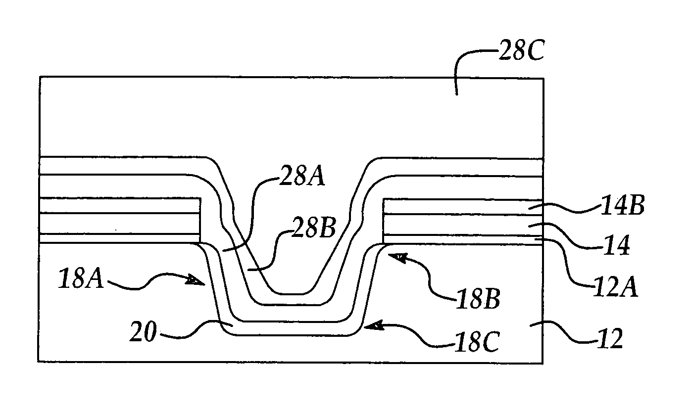
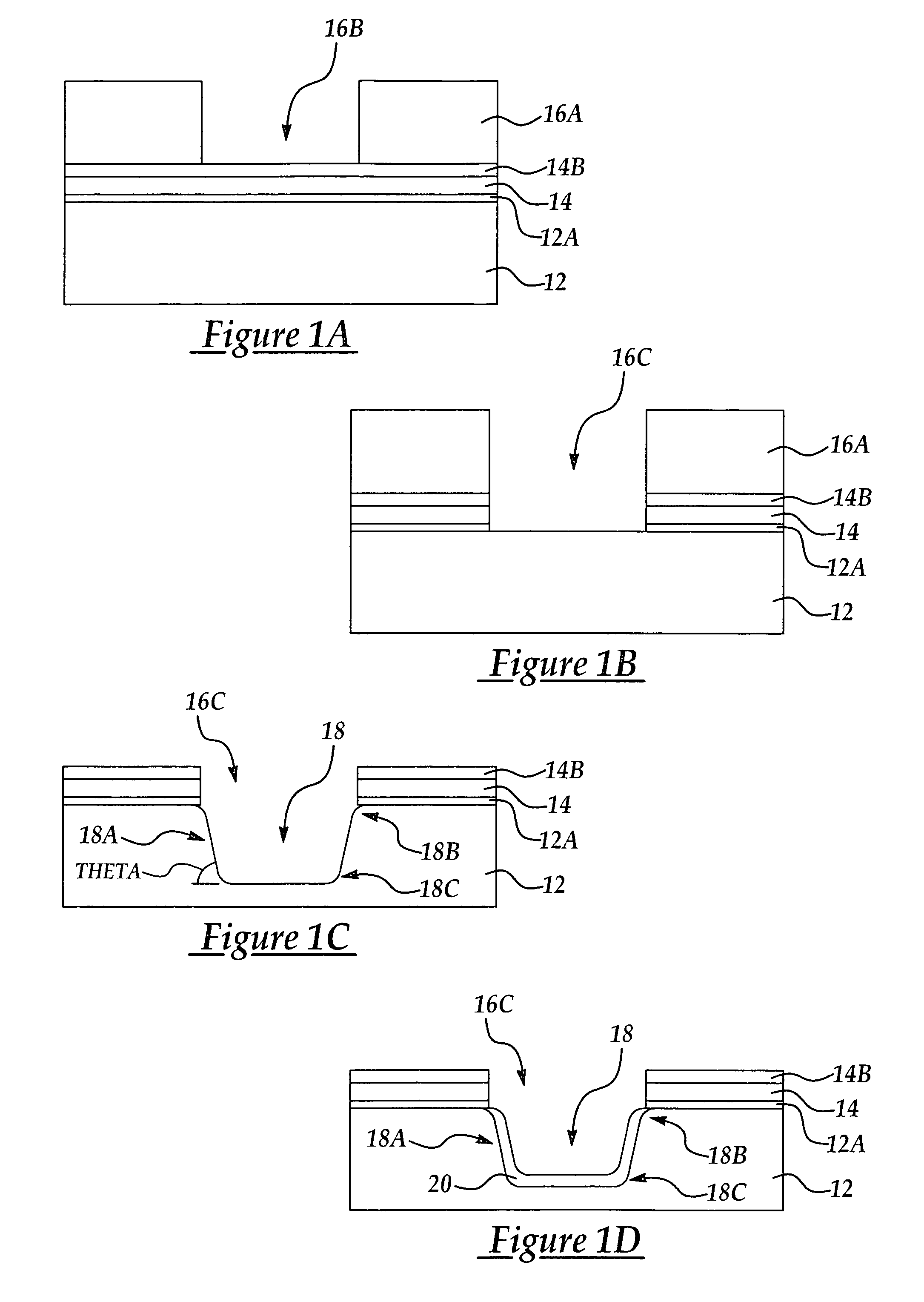
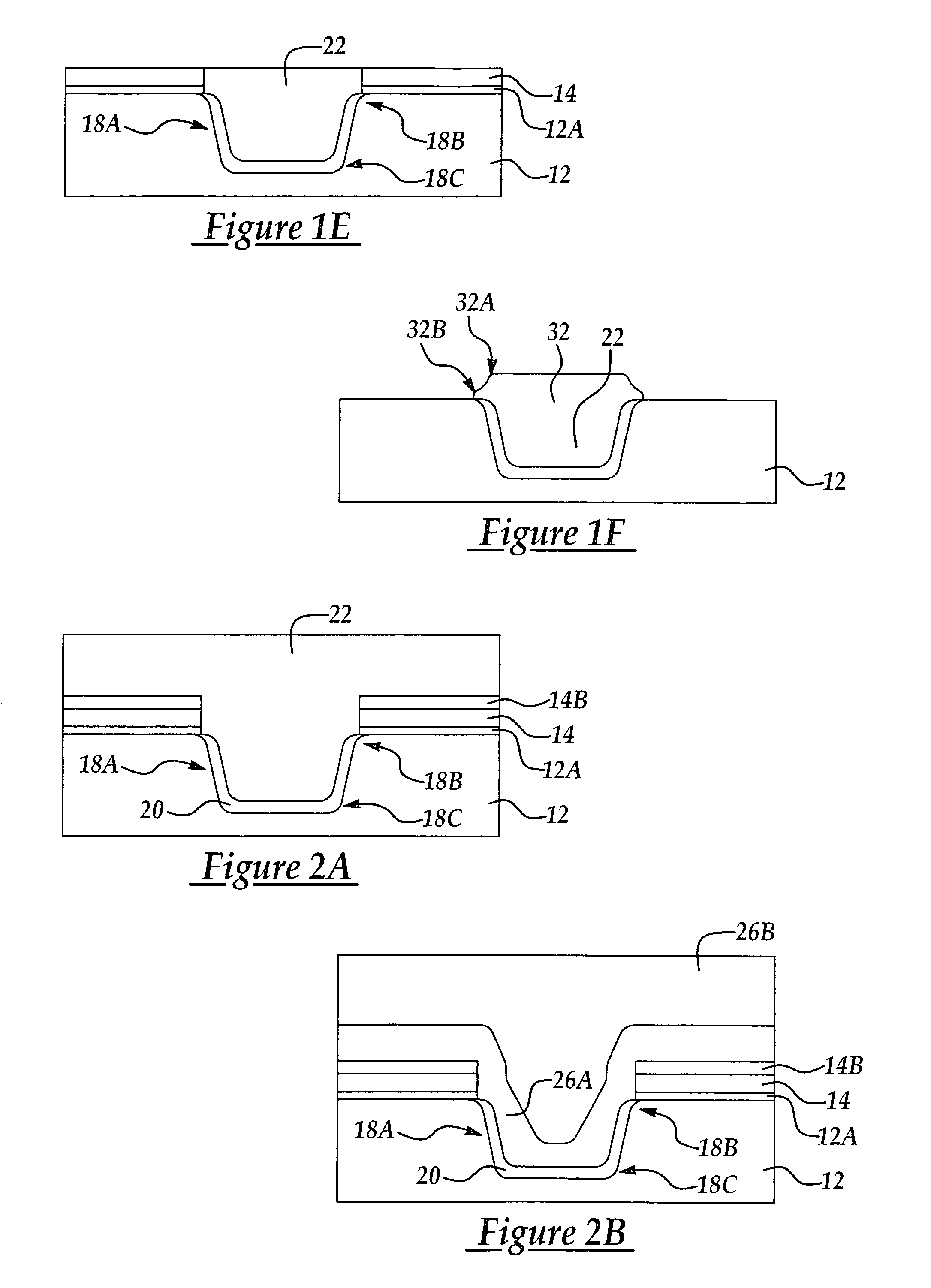
[0014]According to the present invention a method for improved gap fill is explained with reference to the formation of an exemplary shallow trench isolation (STI) feature and exemplary CMOS device. While the method of the present invention is particularly advantageously applied to the formation of STI features, it will be appreciated that the method of the present invention may be applied to the filling of other types of gaps or openings in an integrated circuit manufacturing process where reduced stresses may advantageously improve charge mobility.

[0015]In one exemplary implementation of the present invention, referring to FIG. 1A is shown a semiconductor substrate 12, for example single crystalline or polycrystalline silicon. It will be appreciated that the substrate may include epi silicon layer, buried layers, silicon on insulator (SOI), SiGe, and GaAs. A pad oxide layer 12A of SiO2 about 50 Angstroms to about 150 Angstroms is first thermally grown by conventional processes or ...


PUM


Abstract

A shallow trench isolation (STI) structure and method of forming the same with reduced stress to improve charge mobility the method including providing a semiconductor substrate comprising at least one patterned hardmask layer overlying the semiconductor substrate; dry etching a trench in the semiconductor substrate according to the at least one patterned hardmask layer; forming one or more liner layers to line the trench selected from the group consisting of silicon dioxide, silicon nitride, and silicon oxynitride; forming one or more layers of trench filling material comprising silicon dioxide to backfill the trench; carrying out at least one thermal annealing step to relax accumulated stress in the trench filling material; carrying out at least one of a CMP and dry etch process to remove excess trench filling material above the trench level; and, removing the at least one patterned hardmask layer.

Description

FIELD OF THE INVENTION[0001]This invention generally relates to integrated circuit manufacturing processes and more particularly to an improved shallow trench isolation (STI) formation process and structure to form a STI feature with improved gap filling with reduced stress thereby improving charge carrier mobility.BACKGROUND OF THE INVENTION[0002]As devices become smaller and integration density increases, high density plasma chemical vapor deposition (HDP-CVD) has become a key process due in back filling high aspect ratio features such as shallow trench isolation (STI) features due to its superior gap-filling capability. In particular, high density plasma (HDP) processes, such as electron cyclotron resonance (ECR) processes and inductively coupled plasma (ICP) processes have been found to produce high-quality field oxides. Generally, HDP-CVD provides a high density of low energy ions resulting in higher quality films at lower deposition temperatures, compared to other plasma enhan...

Claims


Application Information

Patent Timeline
Patent Type & Authority Patents(United States)
IPC IPC(8): H01L21/76A61F2/00A61F2/84A61M25/00A61M25/10H01L21/762
CPCA61F2/958H01L21/76235A61M25/001A61M25/0068A61M25/008A61M25/1027A61F2250/0098A61M25/005A61M25/0054A61M25/0069A61M25/0108A61M25/0127A61M2025/1079A61M2025/1093A61M2205/32A61F2002/9583
Inventor FU, CHU-YUNLU, CHIH-CHENGJANG, SYUN-MING
Owner TAIWAN SEMICON MFG CO LTD
Why Eureka
Try Eureka