High voltage lateral FET structure with improved on resistance performance

a lateral fet, high-voltage technology, applied in the direction of transistors, semiconductor devices, electrical equipment, etc., can solve the problems of increasing the cost of chip manufacturing, adversely affecting rsub>on /sub>and vice versa, and adding to cos

Active Publication Date: 2006-10-24
SEMICON COMPONENTS IND LLC
View PDF8 Cites 51 Cited by
  • Summary
  • Abstract
  • Description
  • Claims
  • Application Information

AI Technical Summary

Benefits of technology

[0029]One advantage of the present invention is that n-type regions 16, 18, and 21 provide additional low resistance paths or drift regions for current to flow, which reduces on resistance RON, without increasing the area of device 10. This reduces RON*Area without detrimentally impacting the blocking voltage of device 10 or increasing die or chip size. When under a positive gate bias, gate trench portion 47 causes electrons to accummulate at the interface between layers 16, 18, and 21 and gate trench portion 47 thereby further reducing the resistance in the areas.

Problems solved by technology

One problem with conventional high voltage lateral MOSFETs is that techniques and structures that tend to maximize breakdown voltage (VBD) adversely affect RON and vice versa.
However, these designs require expensive wafer processing involving multiple masking and ion implant steps, very deep diffused body regions or contacts (e.g., 30 to 40 microns deep), and / or expensive silicon on insulator substrates, which increase the cost of chip manufacturing.
Also, these designs are not optimized to support a multitude of blocking voltages, which adds to cost.

Method used


Image

  • High voltage lateral FET structure with improved on resistance performance
  • High voltage lateral FET structure with improved on resistance performance
  • High voltage lateral FET structure with improved on resistance performance

Examples


Embodiment Construction

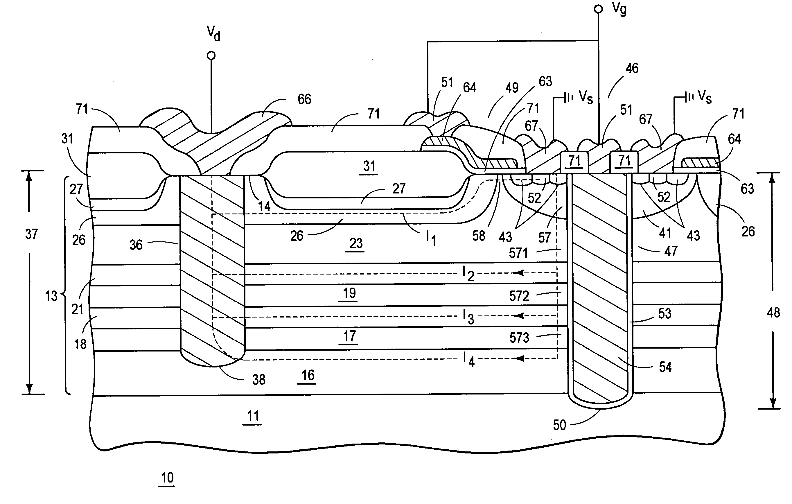
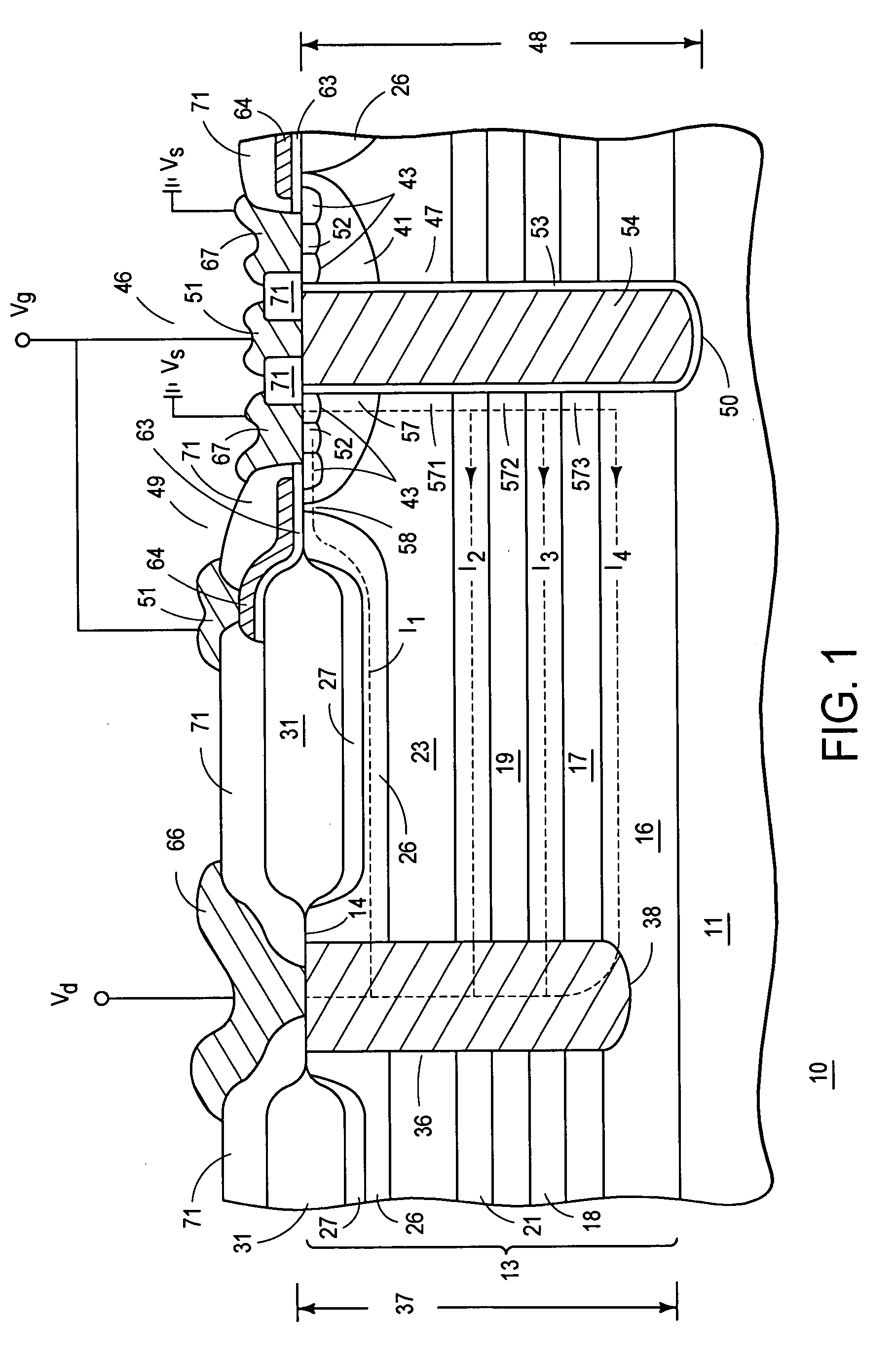
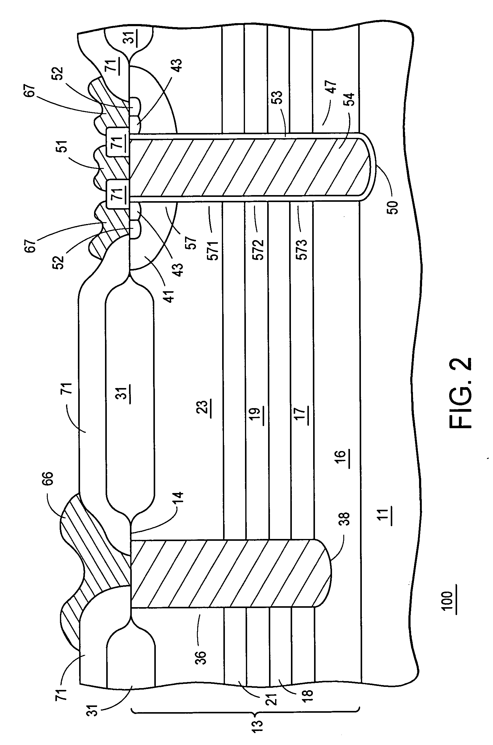
[0011]For ease of understanding, elements in the drawing figures are not necessarily drawn to scale, and like element numbers are used where appropriate throughout the various figures. While the discussion below concerns n-channel devices, the discussion also pertains to p-channel devices, which may be formed by reversing the conductivity type of the described layers and regions. Additionally, although several epitaxial layers are shown in the embodiments, more or less epitaxial layers may be used depending on performance requirements. The embodiment shown is suitable for a blocking voltage on the order of 700 volts.

[0012]FIG. 1 shows a partial cross-sectional view of an insulated gate field effect transistor (IGFET), lateral MOSFET, semiconductor or switching device, structure, or cell 10 having improved RON*Area performance and a high blocking voltage capability. By way of example, MOSFET cell 10 is among many such cells integrated into a semiconductor chip as part of a power inte...


PUM


Abstract

In one embodiment, a lateral FET cell is formed in a body of semiconductor material. The body of semiconductor material includes alternating layers of opposite conductivity type that extend between a trench drain region and a trench gate structure. The trench gate structure controls at least one sub-surface channel region. The body of semiconductor material provides sub-surface drift regions to reduce on resistance without increasing device area.

Description

BACKGROUND OF THE INVENTION[0001]This invention relates generally to semiconductor devices, and more specifically to lateral field effect transistor (FET) structures and methods of manufacture.[0002]Metal-oxide semiconductor field effect transistors (MOSFETs) are a common type of integrated circuit device. A MOSFET device includes a source region, a drain region, a channel region extending between the source and drain regions, and a gate provided over the channel region. The gate includes a conductive gate structure disposed over and separated from the channel regions with a thin dielectric layer.[0003]Lateral MOSFET devices are often used in high voltage (i.e., greater than 200 volts) applications such as off-line switching regulators in AC / DC voltage conversion. Lateral MOSFET devices typically comprise a source region and a drain region separated by an intermediate or drift region. A gate structure is disposed over the channel region of the device. In the on state, a voltage is a...

Claims


Application Information

Patent Timeline
Patent Type & Authority Patents(United States)
IPC IPC(8): H01L29/32H01L29/36H01L29/417H01L29/06H01L29/423H01L29/78H01L29/80
CPCH01L29/0634H01L29/7825H01L29/7816H01L29/7809H01L29/42368
Inventor NAIR, RAJESH S.TU, SHANGHUI LARRYHOSSAIN, ZIAQUDDUS, MOHAMMED TANVIR
Owner SEMICON COMPONENTS IND LLC
Why Eureka
Try Eureka