Method and apparatus for driving low input impedance power transistor switches

a technology of low input impedance and power transistor, applied in the field of electronic circuitry, can solve the problems of additional energy expense, undesirable circuit characteristics, unwanted energy expenditure, etc., and achieve the effects of facilitating variation in drive current, reducing additional energy expense, and improving switch and system performan

Inactive Publication Date: 2006-10-24
NAIR RAJENDRAN
View PDF5 Cites 23 Cited by
  • Summary
  • Abstract
  • Description
  • Claims
  • Application Information

AI Technical Summary

Benefits of technology

[0010]The invention is a novel drive circuit and system architecture that minimizes the additional energy expense in driving power switch devices that require control-input currents and facilitates variation in the drive current for improved switch and system performance.
[0011]In one embodiment of the invention, a current source output replaces the prior art voltage drive circuits and associated external current-limiting resistor. The current-source drive circuit provides both a high impedance as well as variability. The high impedance of the current-source drive circuit enables a reduction in the value of the resistance-bypass capacitor employed in the prior art. The variability in the output current provided by the current-source circuit allows the drive circuits to optimize the control current flowing into the switch device as the characteristics of the switch device change with operating temperature. The drive circuit is capable of providing as output either a desired current, at a high output impedance, or a desired voltage, at a low output impedance, employing a shared amplifier and output transistor. The drive circuit also derives current from the much lower output voltage of the buck conversion system that the invention is used in. This minimizes the static power dissipated in driving the switch, and also minimizes the energy expenditure incurred in increasing the output current to modulate the power switch resistance that increases with increasing temperature.
[0012]In another embodiment of the invention, multiple current sources are employed in parallel to drive the power switch control input, eliminating the need for the external capacitor as well. As in the first embodiment, a current source maintains the power switch in it's ‘ON’ condition by means of a variable current drive, a current source to a voltage reference of the opposite polarity is employed to maintain the device in it's ‘OFF’ state and transient current sources are employed to rapidly transition the power switch device between it's binary states of operation. In this embodiment, the output voltage of the buck conversion system, by definition lower than the input voltage to the system, is employed for the turn-on action of the switch, and an external reference or an internally generated voltage of the opposite polarity is employed to transition to a turn-off mode. Available low-impedance voltage references such as the input power supply to the system and the system ground are employed for the transient drive actions that facilitate rapid transition between the modes.

Problems solved by technology

Static current flow into the control input of a transistor device is, in some applications, an undesirable characteristic of the circuit and an unwanted expenditure of energy.
Maintaining high efficiencies in power supply voltage conversion is critical in such applications due to the costs associated with managing thermal dissipation within the system.
The use of enhancement-mode JFET switches in buck conversion results in additional energy expense (as compared with MOSFET switches) due to the static drive current requirement.
In systems requiring extremely high conversion efficiency, such as battery operated computing devices, or thermally constrained systems, this loss in efficiency makes the JFET-based solution unattractive.
But the presence of resistance R complicates matters in this prior art implementation by decaying this negative charge deposited at the input node of LS back into the signal drive, which is now at the ground potential.
This decay is detrimental in systems employing JFETs because such JFETs may need a constant negative bias at their control gate to maintain the device in its ‘off’ or non-conducting state.
But because systems may desire to reduce the operating frequency to reduce C·V2·f losses in conditions of lower power consumption, this constraint is undesirable.
Also, devices R and C are external components, and because of their large values, may not allow integration into the driver.

Method used


Image

  • Method and apparatus for driving low input impedance power transistor switches
  • Method and apparatus for driving low input impedance power transistor switches
  • Method and apparatus for driving low input impedance power transistor switches

Examples


Embodiment Construction

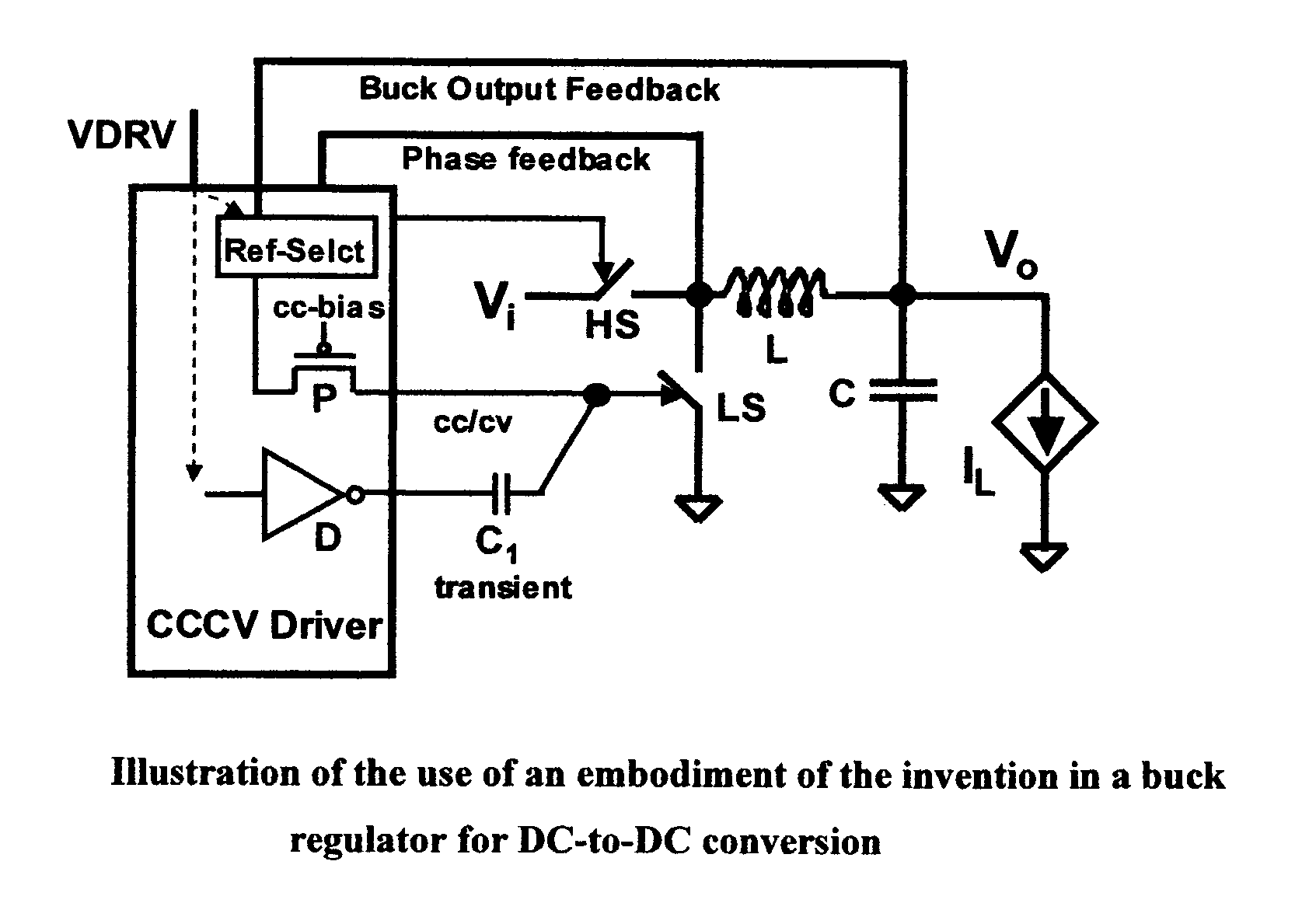
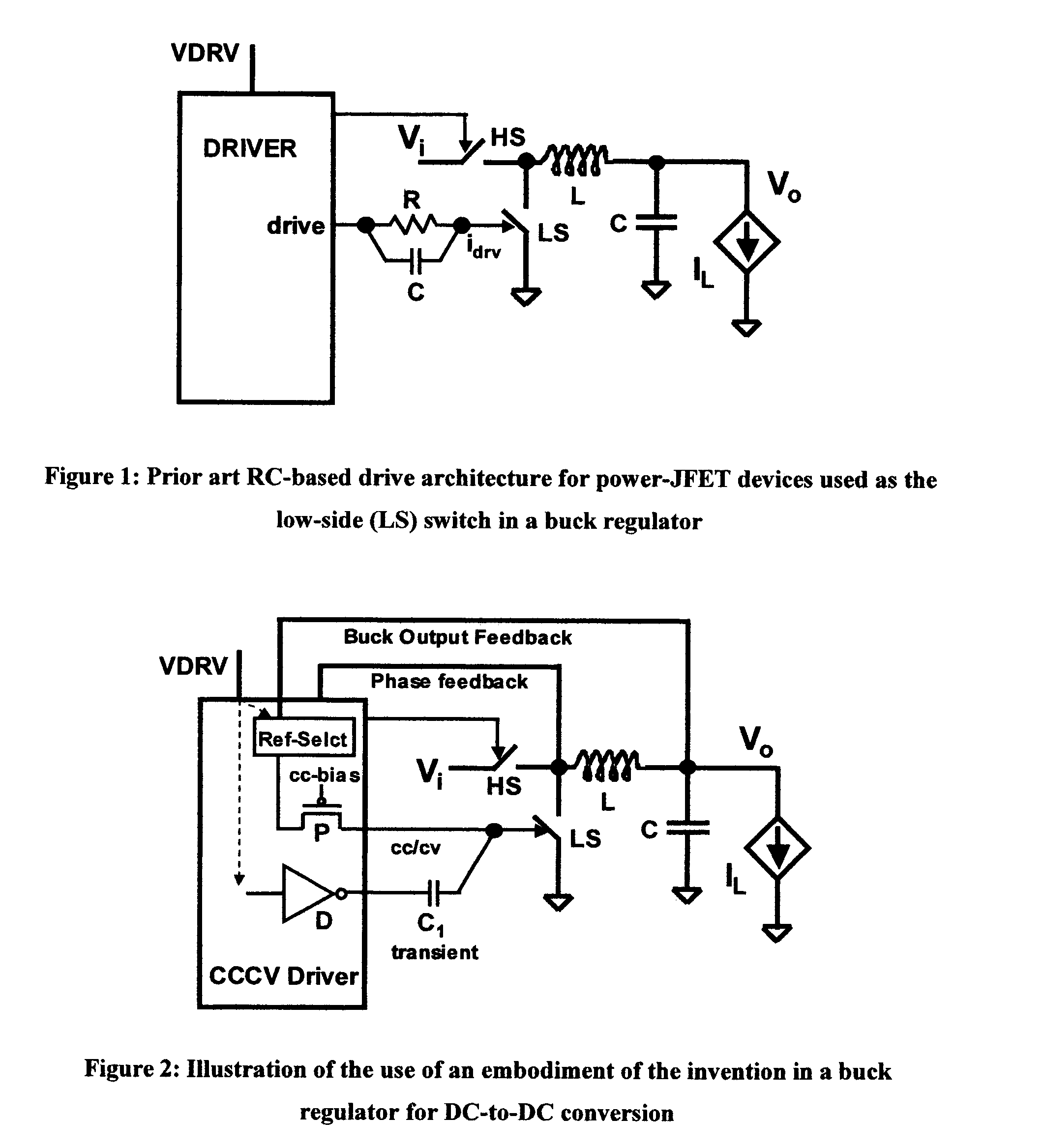
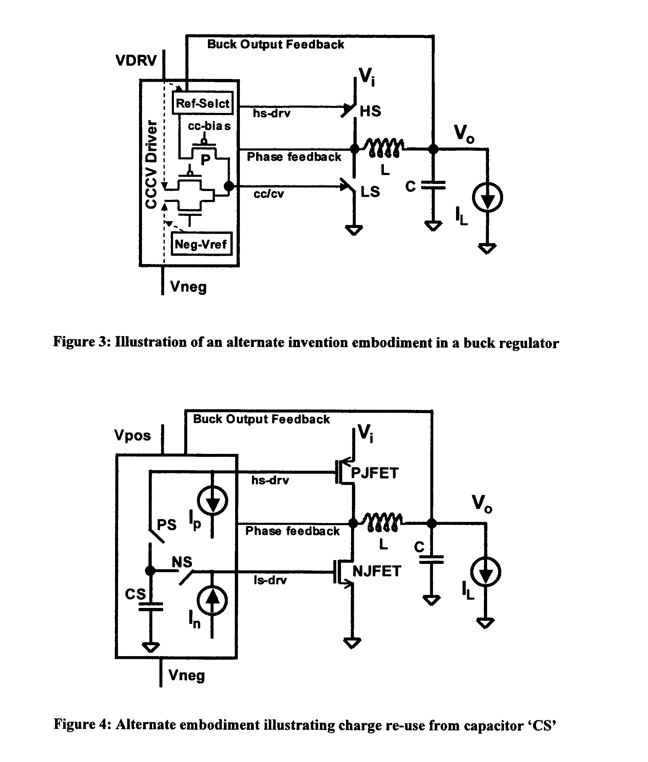
[0018]For purposes of illustration, unless explicitly specified, the description herein will assume that N-type JFET power switches are used, where the channel is formed by electron-donor or n-type semiconductor material and the gate junction is formed by the deposition of p-type material.

[0019]FIG. 1 illustrates prior art drive architecture for the low-side (LS) JFET power switch of a buck converter. A resistor R is employed in series between the output of the driver circuits at node drive and the control gate input of the switch labeled LS. The resistance value of R and the driver power supply value VDRV determine the amount of forward current flowing into the JFET power switch in order to turn it on. One skilled in the art can appreciate that the current flowing into the gate input of the switch is substantially dependent upon the value of the driver power supply, the accuracy and the temperature characteristics of the external resistor as well as the nature of the PN junction of...


PUM


Abstract

An adaptable, low-power drive circuit for transistor switches requiring control input current is disclosed. In one embodiment of the invention, a current source output replaces the prior art voltage drive circuits and associated external current-limiting resistor. The current-source drive circuit provides both a high impedance as well as variability. The high impedance of the current-source drive circuit enables a reduction in the value of the resistance-bypass capacitor employed in the prior art. The variability in the output current provided by the current-source circuit allows the drive circuits to optimize the control current flowing into the switch device as the characteristics of the switch device change with operating temperature. The drive circuit is capable of providing as output either a desired current, at a high output impedance, or a desired voltage, at a low output impedance, employing a shared amplifier and output transistor. The drive circuit also derives current from the much lower output voltage of the buck conversion system that the invention is used in. This minimizes the static power dissipated in driving the switch, and also minimizes the energy expenditure incurred in increasing the output current to modulate the power switch resistance that increases with increasing temperature.

Description

CROSS-REFERENCE TO RELATED APPLICATIONS[0001]1. This application is a continuation of Provisional Patent Application 60 / 460,391 filed on Apr. 7th, 2003, entitled “Method, system and apparatus for constant current constant voltage drive”.[0002]2. The application also relates to invention disclosure document USPTO 528845 dated the 30th of Mar. 2003.TECHNICAL FIELD OF THE INVENTION[0003]Embodiments of the invention relate to electronic circuitry commonly employed to provide regulated voltages to other electronic, electromechanical or electro-optic devices and systems. Such circuitry falls under the broad category of power management electronics.BACKGROUND & PRIOR ART[0004]PN (p-type abutting n-type) semiconductor junctions are ubiquitous in the industry and play a principal role in electronic devices such as Diodes, Silicon-Controlled Rectifiers, Thyristors, Bipolar Junction Transistors (BJTs), Junction Field Effect Transistors (JFETs), and in optoelectronic devices such as Light-Emitt...

Claims


Application Information

Patent Timeline
Patent Type & Authority Patents(United States)
IPC IPC(8): H03K3/00H02M3/158H03B1/00
CPCH02M3/1588Y02B70/1466Y02B70/10
Inventor NAIR, RAJENDRAN
Owner NAIR RAJENDRAN
Why Eureka
Try Eureka