Capacitor and method for producing the same, and circuit board with a built-in capacitor and method for producing the same

Inactive Publication Date: 2006-10-24
PANASONIC CORP
View PDF11 Cites 35 Cited by
  • Summary
  • Abstract
  • Description
  • Claims
  • Application Information

AI Technical Summary

Benefits of technology

[0110]exposing the wiring layer by removing the releasable carrier. This production method also does not require a first circuit board to which the electrolytic capacitor is fixed, and therefore, enables production of a more miniature and thinner circuit board with a built-in capacitor having an improved high-frequency responsibility.
[0111]In any of the above-described methods for producing a circuit board with a built-in capacitor, the conductive adhesive is preferably applied by printing. Printing enables the conductive adhesive to be applied precisely only to a desired position.
[0112]Further, in any of the above-described methods for producing a circuit board with a built-in capacitor, it is preferable that an electrically insulating substrate is prepared wherein one or more through holes are formed in a predetermined position and the hole(s) is filled with a via paste containing electrically conductive powder and a thermosetting resin. The via paste is subjected to a heat treatment at an appropriate time (specifically, at the time when the electrically insulating substrate is superposed so as to form the electrically insulating layer) so that the thermosetting resin is cured to form an inner via. Therefore, this production method including this operation of preparing such a substrate makes it possible to produce a circuit board with a built-in capacitor wherein two wiring layers disposed on both surfaces of the electrically insulating substrate are connected as desired.
[0113]In the case where the through hole(s) is formed in the electrically insulating substrate and the hole(s) is filled with the via paste, the electrolytic capacitor is preferably disposed within the electrically insulating so that the via paste in the through hole contacts with the electrode lead part of the valve metal element for an anode of the capacitor. Thereby, the wiring layer placed on a surface of the electrica

Problems solved by technology

However, when a technique which includes mounting components on a surface of a board is employed, a surface area of the module cannot be smaller than those of the mounted components (that is, the total foot prints of the components).
For this reason, there is a limitation to high-density assembly, even when this technique is employed.
Further, since the components are disposed on a flat surface according to the technique, a connection distance between the components is inevitably longer depending on its constitution, which results in a problem of an increase in loss and an increase in inductance at a high frequency.
However, the capacitor of the above-described configuration tends to be larger in size, since the molding resin and lead frames are disposed around the capacitor element.
For this reason, such a capacitor package does not offer these advantages sufficiently.
When the capacitor is mounted on a wiring layer of a predetermined wiring pattern with solder, solder mounting which is conventionally employed for mounting a chip component cannot be

Method used


Image

  • Capacitor and method for producing the same, and circuit board with a built-in capacitor and method for producing the same
  • Capacitor and method for producing the same, and circuit board with a built-in capacitor and method for producing the same
  • Capacitor and method for producing the same, and circuit board with a built-in capacitor and method for producing the same

Examples


embodiment 1

(Embodiment 1)

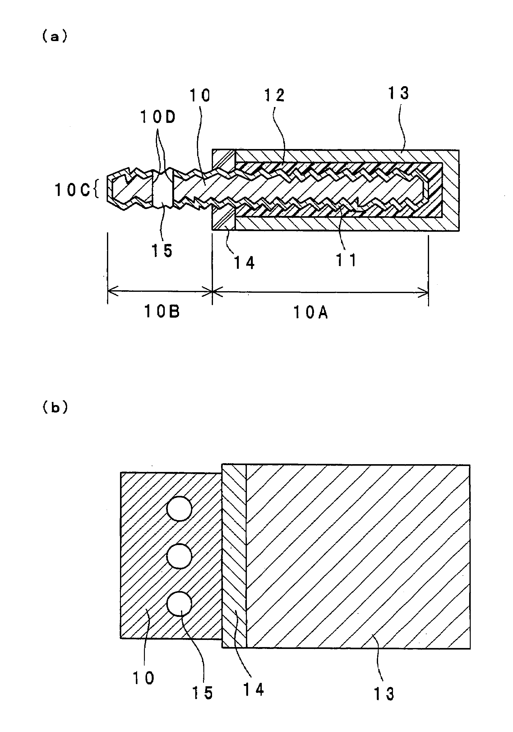
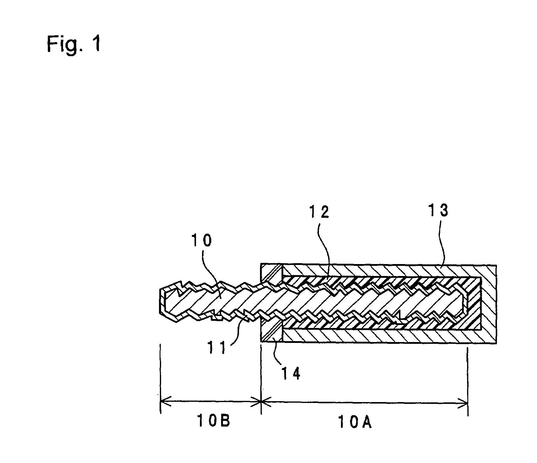
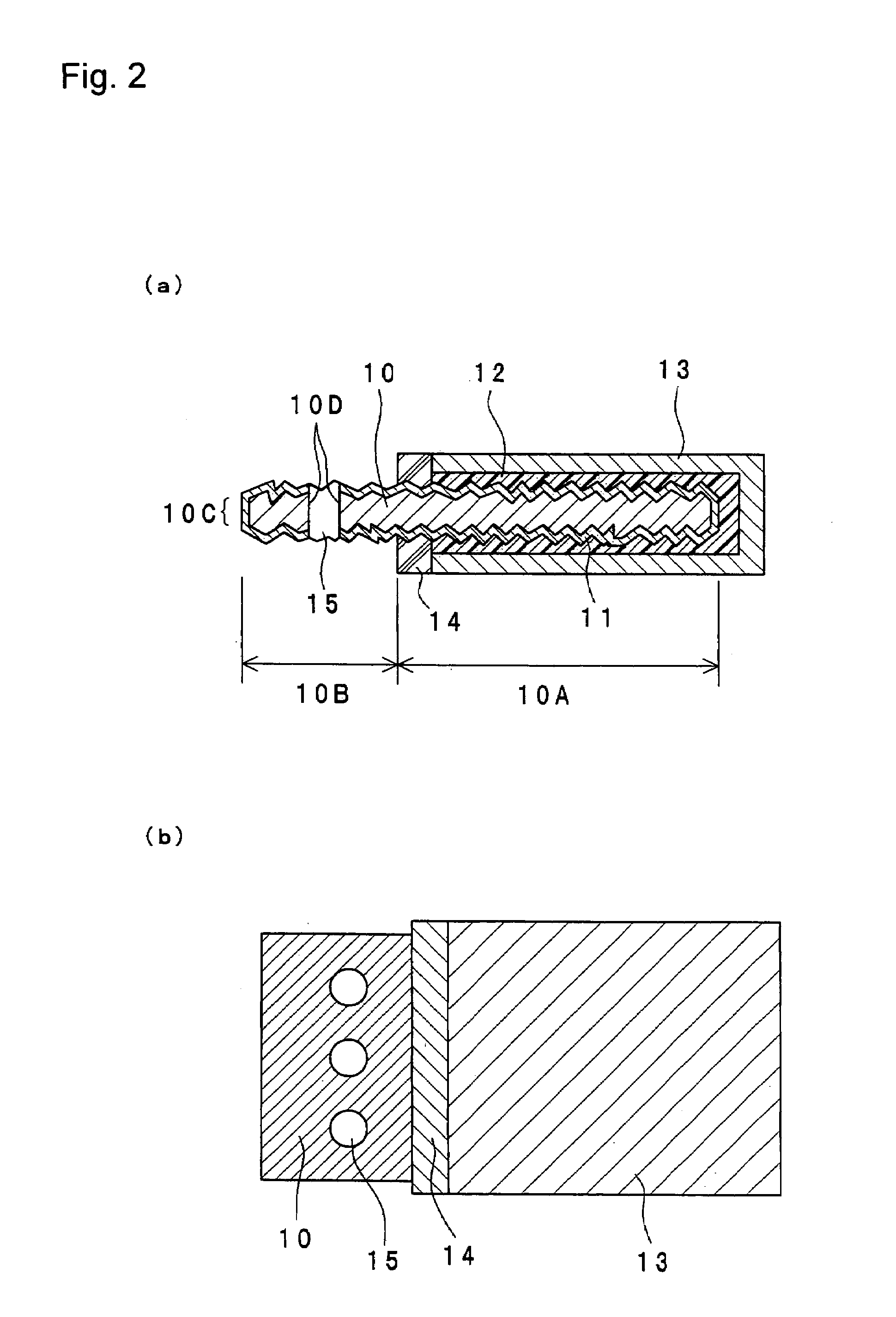
[0141]An embodiment of the electrolytic capacitor of the present invention is shown in FIGS. 2(a) and 2(b). FIG. 2(b) is a plan view of the electrolytic capacitor shown in FIG. 2(a). In FIGS. 2(a) and 2(b), numeral 10C denotes a core of the valve metal element for an anode 10, and numeral 15 denotes a through hole. The inner exposed surface of the through hole 15 except for the portion of the dielectric oxide film 11 corresponds to the core-exposed portion 10D. In FIG. 2, the reference numerals which are identical to those used in FIG. 1 denote identical members or components described with reference to FIG. 1. Therefore, as to those members or components, the detailed description is omitted.

[0142]A method for producing the electrolytic capacitor of this embodiment is described with reference to FIG. 2. Firstly, a metal foil for the valve metal element for an anode is prepared. Herein, a case where an aluminum foil is used, is exemplified.

[0143]Firstly, the aluminum fo...

embodiment 2

(Embodiment 2)

[0148]Another embodiment of the electrolytic capacitor of the present invention is shown in FIG. 3. In FIG. 3, numeral 16 denotes an electrically conductive resin composition containing metal powder and a thermosetting resin, which resin fills the through hole 15 and is electrically connected to the core 10C of the valve metal element for an anode 10. In FIG. 3, the reference numerals which are identical to those used in FIGS. 1 and 2 denote identical members or components described with reference to FIGS. 1 and 2. Therefore, as to those members or components, the detailed description is omitted.

[0149]A method for producing the electrolytic capacitor of this embodiment is described with reference to FIG. 3. Firstly, the electrolytic capacitor with the through hole as shown in FIG. 2 is fabricated by the method as described in connection with Embodiment 1.

[0150]Metal powder and a thermosetting resin are mixed to give an electrically conductive resin composition. The met...

embodiment 3

(Embodiment 3)

[0157]Another embodiment of the electrolytic capacitor of the present invention is shown in FIG. 4. In FIG. 4, numeral 17 denotes an electrically conductive particle. This conductive particle is disposed in the through hole 15 and contacts with the core 10C of the valve metal element for an anode 10 to be electrically connected to the core. In FIG. 4, the reference numerals which are identical to those used in FIGS. 1 to 3 denote identical members or components described with reference to FIGS. 1 to 3. Therefore, as to those members or components, the detailed description is omitted.

[0158]A method for producing the electrolytic capacitor of this embodiment is described with reference to FIG. 4. Firstly, the solid electrolytic capacitor unit of the fundamental configuration as shown in FIG. 1 is fabricated by the method as described in connection with Embodiment 1.

[0159]The conductive particle 17 is prepared of which diameter is larger than the thickness of the valve me...


PUM

PropertyMeasurementUnit
Thicknessaaaaaaaaaa
Dielectric polarization enthalpyaaaaaaaaaa
Electrical conductivityaaaaaaaaaa

Abstract

A miniature solid electrolytic capacitor is provided, which is suitable for being disposed within an electrically insulating layer, and is connected to a component using an electrically conductive adhesive with a connection resistance at an anode being low and with connection reliability being improved. Specifically, the electrolytic capacitor includes a valve metal element for an anode having a capacitor forming part and an electrode lead part, a dielectric oxide film formed on the valve element, a solid electrolyte layer formed on the dielectric oxide film and a charge collecting element for a cathode formed on the solid electrolyte layer, wherein at least one through hole is formed in the electrode lead part so as to expose a core of the valve metal element, and wherein an exposed portion of the core is used as a connecting portion.

Description

CROSS-REFERENCE TO RELATED APPLICATIONS[0001]The present application claims priority under 35 U.S.C. § 119 to Japanese Patent Application No. 2002379231 filed on Dec. 27, 2002, entitled “Capacitor and method for producing the same, and circuit board with a built-in capacitor and method for producing the same.” The contents of that application are incorporated herein by the reference thereto in their entirety.FIELD OF THE INVENTION[0002]The present invention relates to an electrolytic capacitor which can be built in a substrate, a circuit board with the capacitor built-in, and a functional module with the capacitor built-in.BACKGROUND OF THE INVENTION[0003]Recently, as electric and electronic devices have become smaller and more dense, many techniques have been employed wherein a circuit board having a plurality of components is modularized as a package for each functional block, and the necessary modules are combined so as to obtain a predetermined electrical circuit, as a substitut...

Claims


Application Information

Patent Timeline
IPC IPC(8): H01G9/00H01G9/012H05K1/18H05K3/32H05K3/46
CPCH01G9/012H05K1/186H01G4/26Y10T29/417H05K3/4614H05K3/321
Inventor HIRANO, KOICHIYOSHIDA, TSUNENORIHANDA, HIROYUKIYAMASHITA, YOSHIHISANAKATANI, SEIICHI
Owner PANASONIC CORP
Why Eureka
Try Eureka